
File:MicroChipAtomicTrap00.jpg

Original file (890 × 976 pixels, file size: 44 KB, MIME type: image/jpeg)
| This is a file from the Wikimedia Commons. Information from its description page there is shown below. Commons is a freely licensed media file repository. You can help. |
| Description |
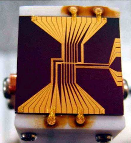
The first microchip atomic trap, designed at the Institute for Laser Science, Japan. The structure of wires is painted with gold at the insulator substrate. The main wire has Z-shape; the magnetic field allows the trapping of neutral atoms due to their magnetic momentum. The ship has sizes 2 x 2 cm. It was placed to the uniform magnetic field (source of this field is not shown in the figure); the traping is realized for so-called "atoms seeking for low magnetic field". The only atoms with positive spin-field energy were trapped. The miminim of the field is realized at the side of the chip, close to the central part of the z-electrode with electric current. This movement is limited by the edges of the "Z". Additional electrodes were designed to allow the play with the effective potential along this wire; the interaction with laser beams and reduction of the trapping potential allow the additional cooling of atoms (coling with vaporation), reaching the BEC. In the current design, the only one additional electrode is supplied with contacts. It was planned to use other electrodes to modify the potential in experiments with single-dimentional quantum mechanics. Actually, more advanced microchip atomic traps were manufactured instead. |
| Date | y.2003 |
| Source | private communication |
| Author | Ken-Ichi Nakagawa |
| Permission (Reusing this file) |
copuleft directly from author |
| Other versions |
Up to my knowkedge, it is the best resolution image of the First Microship Atomic Trap, ever posted. lower resolution pics are available at
|

|
The copyright holder of this file allows anyone to use it for any purpose, provided that the copyright holder is properly attributed. Redistribution, derivative work, commercial use, and all other use is permitted. |
|
|
Links
File history
Click on a date/time to view the file as it appeared at that time.
| Date/Time | Thumbnail | Dimensions | User | Comment | |
|---|---|---|---|---|---|
| current | 03:47, 12 September 2007 | | 890 × 976 (44 KB) | Domitori | {{Information |Description=The first microchip atomic trap, designed at Institute for Laser Science, Japan. The main wire has Z-shape; the magnetic field allows the trapping of neutral atoms due t |
File usage
Global file usage
The following other wikis use this file:
- Usage on es.wikipedia.org
- Usage on fa.wikipedia.org
- Usage on fr.wikipedia.org
- Usage on he.wikipedia.org
- Usage on hr.wikipedia.org
- Usage on it.wikipedia.org