Virtex (FPGA)
Virtex is the flagship family of FPGA products currently developed by AMD, originally Xilinx before being acquired by the former.[1] Other current product lines include Kintex (mid-range) and Artix (low-cost), each including configurations and models optimized for different applications.[2] In addition, AMD offers the Spartan low-cost series, which continues to be updated and is nearing production utilizing the same underlying architecture and process node as the larger 7-series devices.[3]
Virtex FPGAs are typically programmed in hardware description languages such as VHDL or Verilog, using the Xilinx ISE or Vivado computer software.[4]
Xilinx FPGA products have been recognized by EE Times, EDN and others for innovation and market impact.[5][6][7]
Architecture[edit]
The Virtex series of FPGAs are based on Configurable Logic Blocks (CLBs), where each CLB is equivalent to multiple ASIC gates.[8][9] Each CLB is composed of multiple slices, that differ in construction between Virtex families.[9]
Virtex FPGAs include an I/O Block for controlling input/output pins on the Virtex chip, that support a variety of signalling standards.[10] All pins default to "input" mode (high impedance). I/O pins are grouped into I/O Banks, where each Bank can support a different voltage.[10]
In addition to configurable FPGA logic, Virtex FPGAs include fixed-function hardware for multipliers, memories, microprocessor cores, FIFO and ECC logic, DSP blocks, PCI Express controllers, Ethernet MAC blocks, and high-speed serial transceivers.[11][12]
Some Virtex family members (such as the Virtex-5QX) are available in radiation-hardened packages, for outer-space applications.[13]
Families[edit]
Virtex-E[edit]
The Virtex-E family was introduced in September 1999 on a 180 nm process technology.[14] Virtex-E includes a two million system gate device and supports twice the system-gate density and has a 50 percent higher I/O performance than the original Virtex FPGAs.[14][15]
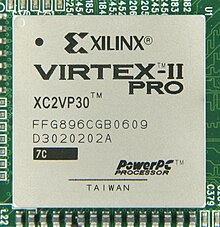
Virtex-II[edit]
Xilinx introduced Virtex-II family in January 2001 on 150 nm process technology,[14] and Virtex-II Pro family in March 2002 on 90 nm process technology.[16] The Virtex-II and Virtex-II Pro families are considered legacy devices, and are not recommended for use in new designs, although they are still produced by Xilinx for existing designs.
Virtex-4[edit]

The Virtex-4 family are considered legacy devices, and are not recommended for use in new designs, although they are still produced by Xilinx for existing designs.
Virtex-4 family was introduced in June 2004 on 90 nm process technology.[17][18] Virtex-4 FPGAs have been used for the ALICE (A Large Ion Collider Experiment) at the CERN European laboratory on the French-Swiss border to map and disentangle the trajectories of thousands of subatomic particles.[19]
Virtex-5[edit]
The Virtex-5 family was introduced in May 2006 on 65 nm process technology.[20] The Virtex-5 LX and the LXT are intended for logic-intensive applications, and the Virtex-5 SXT is for DSP applications.[21] With the Virtex-5, Xilinx changed the logic fabric from four-input LUTs to six-input LUTs. With the increasing complexity of combinational logic functions required by SoC designs, the percentage of combinational paths requiring multiple four-input LUTs had become a performance and routing bottleneck. The new six-input LUT represented a tradeoff between better handling of increasingly complex combinational functions, at the expense of a reduction in the absolute number of LUTs per device. The Virtex-5 series is a 65 nm design fabricated in 1.0 V, triple-oxide process technology.[22][23]
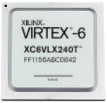
Virtex-6[edit]

The Virtex-6 family was introduced in February 2009 on a 40 nm process technology for compute-intensive electronic systems,[24] and the company claims it consumes 15 percent less power and has 15 percent improved performance over competing 40 nm FPGAs.[25]
Virtex-7[edit]
The Virtex-7 family was introduced in June 2010 on a 28 nm process technology,[26] and is reported to deliver a two-fold system performance improvement at 50 percent lower power compared to previous generation Virtex-6 devices.[27] In addition, Virtex-7 doubles the memory bandwidth compared to previous generation Virtex FPGAs with 1866 Mbit/s memory interfacing performance and over two million logic cells.[28][29]
Virtex-7 (3D)[edit]
In 2011, Xilinx began shipping sample quantities of the Virtex-7 2000T FPGA, which combines four smaller FPGAs into a single package by placing them on a special silicon interconnection pad (called an interposer) to deliver 6.8 billion transistors in a single large chip. The interposer provides 10,000 data pathways between the individual FPGAs – roughly 10 to 100 times more than would usually be available on a board – to create a single FPGA.[30][31][32] In 2012, using the same 3D technology, Xilinx introduced initial shipments of their Virtex-7 H580T FPGA, a heterogeneous device, so called because it comprises two FPGA dies and one 8-channel 28Gbit/s transceiver die in the same package.[33]
As Xilinx introduced new high capacity 3D FPGAs, including Virtex-7 2000T and Virtex-7 H580T products, these devices began to outpace the capacity of Xilinx’s design software, which led the company to completely redesign its tool set. The result was the introduction of the Vivado Design Suite, which reduces the time needed for programmable logic and I/O design, and speeds systems integration and implementation compared to the previous software.[4][34]
Virtex UltraScale[edit]
The Virtex UltraScale family was introduced in May, 2014 on a 20 nm process technology.[35][36] The UltraScale is a "3D FPGA" that contains up to 4.4M logic cells, and uses up to 45% lower power vs. previous generations, and up to 50% lower BOM cost.[37]
Virtex UltraScale+[edit]
The Virtex UltraScale+ family was introduced in January 2016 on a 16 nm process technology.[38]
SoC[edit]

The Virtex-II Pro, Virtex-4, Virtex-5, and Virtex-6 FPGA families, which include up to two embedded IBM PowerPC cores, are targeted to the needs of system-on-chip (SoC) designers.[39][40][41]
See also[edit]
References[edit]
- ^ "Xilinx Inc, Form 10-K, Annual Report, Filing Date May 15, 2017". secdatabase.com. Retrieved May 6, 2018.
- ^ DSP-FPGA.com. Xilinx FPGA Products.” April 2010. Retrieved June 10, 2010.
- ^ Company Release. “Xilinx Announces the Spartan-7 FPGA Family.” Nov 19, 2015. Retrieved February 10, 2015.
- ^ a b Brian Bailey, EE Times. "Second generation for FPGA software." Apr 25, 2012. Retrieved Dec 21, 2012.
- ^ EE Times, “EE Times 2010 ACE Award for Design Innovation Archived 2010-06-14 at the Wayback Machine.” April 27, 2010. Retrieved June 17, 2010.
- ^ EDN, “EDN Hot 100 Products of 2007: Digital, Memory and Programmable ICs Archived 2012-04-03 at the Wayback Machine.” December 14, 2007. Retrieved June 17, 2010.
- ^ EDN, “The Hot 100 Electronic Products of 2009 Archived 2012-04-03 at the Wayback Machine.” December 15, 2009. Retrieved June 15, 2010.
- ^ Field Programmable Logic and Applications, Springer Science & Business Media, 21-Aug-2002
- ^ a b Handbook of Signal Processing Systems - Volume 2, Springer Science & Business Media, 20-Jun-2013
- ^ a b Cryptographic Hardware and Embedded Systems, Springer Science & Business Media, 02-Sep-2003
- ^ Ron Wilson, EDN. "Xilinx FPGA introductions hint at new realities Archived 2011-05-25 at the Wayback Machine." February 2, 2009 Retrieved June 10, 2010.
- ^ Design & Reuse. "New Xilinx Virtex-6 FPGA Family Designed to Satisfy Insatiable Demand for Higher Bandwidth and Lower Power Systems." February 2, 2009. Retrieved June 10, 2010.
- ^ Don Clark, Wall Street Journal. "Xilinx Say New Chips Adept at Surviving Space Radiation." July 19, 2010. Retrieved August 10, 2010.
- ^ a b c "Xilinx Inc, Form 10-K, Annual Report, Filing Date Jun 12, 2001". secdatabase.com. Retrieved May 6, 2018.
- ^ "Xilinx Inc, Form 10-K, Annual Report, Filing Date Jun 4, 2004". secdatabase.com. Retrieved May 6, 2018.
- ^ "Xilinx Inc, Form 10-K, Annual Report, Filing Date Jun 17, 2002". secdatabase.com. Retrieved May 6, 2018.
- ^ "Xilinx Inc, Form 10-K, Annual Report, Filing Date Jun 1, 2005". secdatabase.com. Retrieved May 6, 2018.
- ^ "Xilinx Inc, Form 8-K, Current Report, Filing Date Oct 21, 2004" (PDF). secdatabase.com. Retrieved May 6, 2018.
- ^ Xcell Journal, "CERN Scientists Use Virtex-4 FPGAs for Big Bang Research Archived 2009-03-27 at the Wayback Machine." July 2008. Retrieved January 28, 2009.
- ^ "Xilinx Inc, Form 8-K, Current Report, Filing Date Jul 26, 2006". secdatabase.com. Retrieved May 6, 2018.
- ^ DSP DesignLine. "Analysis: Xilinx debuts Virtex-5 FXT, expands SXT." June 13, 2008. Retrieved January 20, 2008.
- ^ "Xilinx Inc, Form 10-K, Annual Report, Filing Date May 31, 2006". secdatabase.com. Retrieved May 6, 2018.
- ^ National Instruments. "Advantages of the Xilinx Virtex-5 FPGA." June 17, 2009. Retrieved June 29, 2010.
- ^ "Xilinx Inc, Form 10-K, Annual Report, Filing Date Jun 1, 2009". secdatabase.com. Retrieved May 6, 2018.
- ^ Company Release. "New Xilinx Virtex-6 FPGA Family Designed to Satisfy Insatiable Demand for Higher Bandwidth and Lower Power Systems." February 2, 2009. Retrieved February 2, 2009.
- ^ "Xilinx Inc, Form 10-K, Annual Report, Filing Date May 31, 2011". secdatabase.com. Retrieved May 6, 2018.
- ^ "Xilinx Inc, Form 8-K, Current Report, Filing Date Jul 21, 2010". secdatabase.com. Retrieved May 6, 2018.
- ^ EE Times. “Xilinx Announces the Spartan-7 FPGA Family.” Nov 19, 2015. Retrieved February 10, 2015.
- ^ Kevin Morris, FPGA Journal. “Veni! Vidi! Virtex! (and Kintex and Artix Too) Archived 2010-11-23 at the Wayback Machine.” June 21, 2010. Retrieved September 23, 2010.
- ^ Don Clark, The Wall Street Journal. "Xilinx Says Four Chips Act Like One Giant." October 25, 2011. Retrieved November 18, 2011.
- ^ Clive Maxfield, EETimes. "Xilinx tips world’s highest capacity FPGA." October 25, 2011. Retrieved November 18, 2011.
- ^ David Manners, Electronics Weekly. "Xilinx launches 20m ASIC gate stacked silicon FPGA." October 25, 2011. Retrieved November 18, 2011.
- ^ Electronic Product News. "Interview with Moshe Gavrielov, president, CEO, Xilinx." May 15, 2012. Retrieved June 12, 2012.
- ^ EDN. "The Vivado Design Suite accelerates programmable systems integration and implementation by up to 4X." Jun 15, 2012. Retrieved Jan 3, 2013.
- ^ "Xilinx Inc, Form 10-K, Annual Report, Filing Date May 13, 2015". secdatabase.com. Retrieved May 6, 2018.
- ^ http://forums.xilinx.com/t5/Xcell-Daily-Blog/Xilinx-ships-first-20nm-Virtex-UltraScale-FPGA-Why-this-matters/ba-p/458488 [user-generated source]
- ^ Virtex UltraScale, Xilinx
- ^ "Xilinx Inc, Form 10-K, Annual Report, Filing Date May 17, 2016". secdatabase.com. Retrieved May 6, 2018.
- ^ Virtex-II Pro Datasheet
- ^ Virtex-4 Family Overview
- ^ Richard Wilson, ElectronicsWeekly.com, "Xilinx repositions FPGAs with SoC move." February 2, 2009. Retrieved on February 2, 2009.
Alternative FPGA manufacturers[edit]
- Intel (former Altera)
- Lattice Semiconductor
