
Talk:Emitter-coupled logic/Archive 2
| This is an archive of past discussions. Do not edit the contents of this page. If you wish to start a new discussion or revive an old one, please do so on the current talk page. |
| Archive 1 | Archive 2 |
Explanation
This once well-written article has been continuously edited by one individual for 4 months. The circuit diagram next to the new Explanation section is not an ECL circuit. What purpose does it serve? I think the edits of the past 4 months, which are all by 1 user, should be undone and the article reverted. Zen-in (talk) 04:40, 28 September 2009 (UTC)
- Are you referring to the edits by Circuit-fantasist within the last 9 days, or something else? I agree that not everything he has done was right (I reverted only a bit of it), but I haven't studied it in detail. Be specific about what's wrong, or fix it, or revert to what you think was a better state, and we'll have something to discuss. See WP:BRD. Dicklyon (talk) 04:59, 28 September 2009 (UTC)
- Zen-in, you've removed Circuit-fantasist's explanation with edit summary saying it's "confusing". This is not an adequate response to my suggestion to tell us what's wrong with it, so I've reverted that removal. I'm not saying it's great, but it's worth discussing so we can get to a better version, yes? Dicklyon (talk) 18:21, 18 October 2009 (UTC)
- The circuit diagram next to the explanation section is not a good representation of an ECL gate. Instead of being one gate it is actually one gate plus the output stages of two preceding gates (or something like that). I have seen better schematics and even if this schematic was technically OK it is not in an acceptable format. With a better schematic the explanation section could be made shorter and more concise. I don't think 500-600 words are needed here. Of course once you replace the schematic the description has to go as well. I have been asked to not edit this page any more and have agreed to this request. You asked for my input and so my suggestion is to replace the photo of the whiteboard with a better schematic in an acceptable format. Then, once you have a better schematic with just 4 or 5 transistors (4 BJT = NOT, 5 BJT = OR or NOR, 6 BJT = OR and NOR with differential outputs) and realistic resistor values the analysis becomes relatively simple, requiring 100-150 words. Zen-in (talk) 22:46, 18 October 2009 (UTC)
- Thanks for your comments. I agree the explanation is long-winded, and the diagram is somewhat confusing until you realize that the shaded blue region on the left represents, as it says on it, a "driving stage" providing input to the 5-transistor NOR gate. I don't think it's a whiteboard photo, but a pretty carefully done drawing. I still haven't quite worked out what all the voltage lines and annotations are trying to say. If you can suggest or provide a better drawing, and suggest a better explanation, I'll try to broker a collaborative compromise. Dicklyon (talk) 01:11, 19 October 2009 (UTC)
- Looking at the diagram again I see it isn't a whiteboard photo but is a photo of a drawing. In any case there has been some discussions concerning the suitability of these photos since they can't be modified. It could be sent through WP:GL/I but there are no values to the resistors, is overly busy, and is not a good representation of an ECL gate. For those reasons it is technically a dead-end. There is a good schematic and circuit description in one of my EE textbooks. I'll see if I can create an SVG format schematic and re-write the description of it. The other alternative is to use the Motorola ECL 10k circuit diagram as a basis for the explanation. I can also write an explanation section using it, but the example I have is a better choice. Zen-in (talk) 02:09, 19 October 2009 (UTC)
- I agree the form of the schematic is not ideal, but I think it's creative, carefully done, correct, and essentially identical to the MECL 10K diagram at the lead. The resistor values are not at all critical to an understanding of how it works. If you can make a clean alternative svg, I can work with that. Dicklyon (talk) 05:16, 19 October 2009 (UTC)
DC drift of output
It seems to me that another disadvantage ECL might be that the output voltage of each depends on variables such as the resistor values, and these will tend to accumulate after several stages. This is unlike other logic families that switch from fully on to fully off. Maybe this isn't a problem for a low input if the input transistors are cut-off, but it might be for a high input. Do ECL gates need to be fine-tuned to ensure the high-level voltages stay within reasonable limits? 60.241.12.136 (talk) 08:19, 18 October 2009 (UTC)
- It's so wonderful to see that some (even anonymous) wikipedian want not only to convey else's knowledge but to think and discuss circuit phenomena relying on his/her own mind! I admire your speculation and will join this discussion. Please, look first at the previous version and especially on the figure on the right; maybe you will find the answer by yourself. Circuit-fantasist (talk) 09:30, 18 October 2009 (UTC)
- I undid the removal of your explanation (see above), so we can discuss it as I suggested before. Dicklyon (talk) 18:24, 18 October 2009 (UTC)
- Thank you, Dicklyon. I realize that some of my insertions are lengthy; others are not backed up with quotations enough and my style is not so elegant:) But I hope they are true and may be corrected and improved by you and other wikipedians contributing this page. I am ready to clarify and discuss them. As I can see from your last edit of the caption, you prefer to express thoroughly your thoughts and arrange them in a logical succession. According to this approach, Explanation should consist of three sub-sections: basic idea, implementation (circuit structure) and operation (at input logical "0" and "1"). We may use the same or simpler structure in DTL, TTL and CMOS logic as well. Circuit-fantasist (talk) 21:14, 18 October 2009 (UTC)
- I undid the removal of your explanation (see above), so we can discuss it as I suggested before. Dicklyon (talk) 18:24, 18 October 2009 (UTC)
- The errors due to resistor tolerances and the like will not accumulate because in normal quiescent* operation, the differential amplifier (also called the current switch) will have all the current in the left side, or all the current in the right side, regardless of any minor variations in the inputs.
- I agree; the voltages (output levels and input thresholds) are set by the transistor VBEs, which are pretty stable, and temperature compensated by the diodes, and by some not-very-critical resistor dividers; resistance ratios are also very stable in ICs. It's a very robust logic family, and many large computer systems were built with it, with no particular difficulties. It has lots of margin for noise and component variations. Dicklyon (talk) 18:24, 18 October 2009 (UTC)
- I think the key phrase in 60.241.12.136's question is "these will tend to accumulate after several stages." This is characteristic of analog circuitry, where the errors in each successive stage make the signal worse and worse. Digital circuits, on the other hand, when they switch properly, virtually destroy all evidence of tolerances in the input, and output a level that for practical purposes depends only on whether the circuit is in the 1 state or the 0 state. So the question is, what part of ECL makes it behave in a binary fashion. That part is the differential amplifier. It is designed (to take all inputs in the low level as an example) so that when all inputs are at the "least negative down level" under worst case operating conditions, the input side of the differential amp will not be conducting any current. Any further decrease in the inputs, to the nominal down level, or the "most negative down level", will not make any difference in the output. --Jc3s5h (talk) 01:39, 19 October 2009 (UTC)
Thanks for all your responses. I found the answer myself after some googling. jc3s5 is right that my concern was the propagation and accumulation of noise after each stage. But I already understood that the input transistor would cut-off when the input below the lower threshold and prevent the propagation of noise in the Low state. I was asking how the HIGH level was stabilized without saturating the transistor. What I didn't understand then was that raising the input above the High threshold would then cut-off the OTHER transistor (the one attached to the constant-voltage bias and the output). This effectively forces the output to stay at a maximum level defined by the components of that gate, independently of the input voltage provide it remains above the High threshold. The clever thing about ECL is that it replaces cut-off & saturation in 1 transistor with cut-off in 2 opposing transistors.
I guess I was confused by the input transistors being described as Differential Amplifier. Yes, it is that too, but actually it is a Voltage Comparator. There isn't necessarily any difference between the two circuits - rather it's how they are used. For a DA, you don't want the gain so high that the output is clipped, but for a VC you do. In this case you do, to ensure the output remains stable in spight if small input changes.
When thinking of the gate as a DA and Voltage Shifter, it just seemed obvious that every little change in the input would be propagated like an analog system.
Even so, I did find some references to the problems of drift in ECL circuits and how to solve them. The problem is not as bad as I thought but it does exist, just because the margin between High and Low is so small.
BTW, I agree that the new explanation and diagram are very complicated. I already understood the idea of Diff Amps from the article on that, and maybe a detail explanation belongs there rather than here. 60.241.12.136 (talk) 10:24, 19 October 2009 (UTC)
Although each gate is able to produce output signals that are unaffected by small variations of the input voltages, it is still important to limit the input voltage to avoid saturating the input transistor because that would slow down the switch. After all, the whole point of ECL is to avoid saturation delays. 60.241.12.136 (talk) 10:02, 12 November 2009 (UTC)
- The input transistor T1 will saturate (VCE1 = 0 V) when VRE5' = VEE.RE/(RE + RC1) + VBE1. If we replace the emitter resistor RE with a constant current source IE, the output voltage VC1 will become less sensitive against the input voltage variations and T1 will saturate when VRE5' = VEE - IE.RC1 + VBE1. Here is another more colorful and figurative explanation for this situation (when the input voltage reaches VH and continues "moving" up):
- In the emitter resistor case, the emitter voltage "moves" up with the same rate as the input voltage while the collector voltage VC1 "moves" down with a slower rate (the two voltages "move" in opposite directions).
- In the emitter constant current source case, the emitter voltage "moves" up with the same rate while the collector voltage VC1 does not "move" at all (the two voltages "move" slowly in opposite directions).
- In comparison with the opposite situation during the transition (with a relatively constant voltage source inserted in the emitter), the emitter voltage "moves" up with a slower rate than the input voltage while the collector voltage VC1 "moves" down vigorously (the two voltages "move" impetuously in opposite directions). Circuit dreamer (talk) 17:57, 12 November 2009 (UTC)
Why are the collector resistors different?
I'd like to pose another question to make the discussion above even more interesting. Look at Motorola ECL 10,000 circuit diagram: Q2 has a 220 Ω collector resistor while Q3 has a 245 Ω collector resistor. Why are the two resistances different? Circuit-fantasist (talk) 21:46, 18 October 2009 (UTC)
- How does that make it more interesting? Are you setting a puzzle for us? Do you know the answer? I suspect it's about optimizing the noise margin for the gate. Dicklyon (talk) 01:13, 19 October 2009 (UTC)
- If you assume Q2 and Q3 have the same characteristics what difference does it make if the resistors have different values? Is there a difference in how the two transistor circuits operate and if so what is the difference? Zen-in (talk) 14:50, 19 October 2009 (UTC)
- This is answered on pages 2 and 3 of the MECL System Design Handbook, new revised editon (1972). For MECL 10,000, when all the inputs are at a 0 logic level (using positive logic), the more positive end of the 779 Ω resistor is about -2.09 V and the resistor current is about 4 mA. The voltage at the more negative end of the 245 Ω resistor is about -0.98 V.
- If one or more inputs is a nominal logic 1 (-0.924 V), the more positive end of the 779 Ω resistor is about -1.74 V and the resistor current is about 4.49 mA. The voltage at the more negative end of the 220 Ω resistor is about -0.98 V. We see that the 0 output level will be nominally the same for both sides of the differential amplifier. If the resistors had been the same, the 0 output level for the left side of the differential amp would have been more negative than the right side. --Jc3s5h (talk) 20:45, 19 October 2009 (UTC)
- I agree. The low output voltage (logical "0") depends on the current flowing through the collector resistor and on the very resistance (VRC = IC x RC). Different resistances can compensate different currents to obtain the same voltage drops (equal low output voltages). Circuit-fantasist (talk) 20:57, 19 October 2009 (UTC)
- I suggest another (simpler) explanation. The two input transistors (T1 and T3) act as voltage-controlled current sources with the same emitter resistor RE but with slightly different input voltages (4.3 V and 3.9 V). They determine different currents (4.5 mA and 4 mA) that, flowing through the different resistances (220 Ω and 245 Ω), cause the same output voltages (1 V). Circuit-fantasist (talk) 21:34, 19 October 2009 (UTC)
- Jc3s5h's answer is
partlyright. CML circuits do not havetheequal output levels if the collector resistors are the same value. The different resistor values make the output levels the same - because of IR and gmR (gain). If the output levels were not the same, the level shifters (Q5 and Q6 shift the output by one Vbe drop, whenthe rightpull-down resistors are added, so the gates can be cascaded) would not have the same logic 1 level. Circuit dreamer's second explanation (intuitive?) is right. Zen-in (talk) 22:05, 19 October 2009 (UTC)
- Jc3s5h's answer is
So the resistors are not the same because, although you want the outputs to mirror each other the inputs do not. Unlike a Diff Amp with balance inputs and outputs, here you have a single-ended input and a fixed voltage input - not symmetrical. Then I ask my self - why is it so important for the outputs to mirror each other? The reason for that is it is easier to build a system out of many of these gates if both output have the same levels. Another may be lower noise emission if the total voltage of both outputs is constant. 60.241.12.136 (talk) 09:57, 12 November 2009 (UTC).
- I like your manner of reasoning. During the transition, an ECL gate is an emitter-coupled amplifier (a differential amplifier with the one steady and the other varying input voltage). In this case it is a symmetrical circuit, whose two output voltages "move" in opposite directions with the same rate. At the ends (logical "0" and "1"), an ECL gate is neither a differential amplifier nor an emitter-coupled amplifier. In this case, it is completely nonsymmetrical as it is divided into two independent parts (devices) - a pull-up resistor and an emitter-degeneration amplifier with a constant input voltage. In regard to the input voltage, these devices change (swap) their place. The problem is that when the right leg behaves as an emitter-degeneration amplifier, the input voltage is -1.3 V and when the left leg behaves as an emitter-degeneration amplifier, the input voltage is -0.9 V. But the output voltages for the two cases must be equal because we may use either voltage as an input to another ECL gate. That's why we have to equalize them by different collector resistances. Circuit dreamer (talk) 18:44, 12 November 2009 (UTC)
- One reason for keeping all the low outputs as consistent as possible is that when the logic state changes to a high level, it will take longer to raise a level than is lower than necessary to the high level. This will result in a longer worst-case propagation delay, and will make the propagation delay less predictable. This problem occurs even
ifthough the reference transistor does not go into saturation.if the reference transistor saturates, the problem goes from being an annoying problem to making the delays so long that a reasonable system design becomes impractical.--Jc3s5h (talk) 18:46, 12 November 2009 (UTC) Modified at 21:16 UT.
- Your thought about preventing the input voltage from dropping below VL is valuable. But you make me reason what can make the reference transistor saturate as it is separated from the input part - resistance tolerances of R1, R2, RE, RC3, thermal variations, excessive load connected to T3's collector, something else...? T3 β tolerances cannot cause saturation as they are suppressed by the series negative feedback (emitter degeneration). Circuit dreamer (talk) 19:02, 12 November 2009 (UTC)
- The input voltage would not have any effect that might cause the reference transistor to saturate; I should have had some more coffee before I made my comment. --Jc3s5h (talk) 21:18, 12 November 2009 (UTC)
- I agree. The input voltage (the input transistor T1 or T2) can only make T3 become cut-off but it cannot saturate T3. If it tries to saturate T3, it will be disconnected from T3. BTW, it would be very interesting to consider the fully symmetrical ECL with differential input. Circuit dreamer (talk) 21:46, 12 November 2009 (UTC)
- The input voltage would not have any effect that might cause the reference transistor to saturate; I should have had some more coffee before I made my comment. --Jc3s5h (talk) 21:18, 12 November 2009 (UTC)
- Differential current switch was used; see U.S. patent 4,967,151. I don't have a citation, but I happen to know that unlike many patents, that one went into production. --Jc3s5h (talk) 23:56, 15 November 2009 (UTC)
Shunt resistance at the common node increases inverting gain and decreases non-inverting gain. In ECL families where a resistor sets tail bias for the differential amp, the common-mode rejection is poor enough that unbalanced inputs lead to poorly balanced outputs. But (outside of Motorola) other ECL families (100K for example, and LSI) used a single-BJT active current source in the tail so their load resistors were the same.Prari (talk) 23:19, 12 November 2009 (UTC)
- Interesting thought... I'll only enlarge this speculation to clarify the powerful idea. The problem of the simple "resistor current source" is that it is controlled by two different input voltages - once from T3's base (the reference voltage) and second time from T1's base (the input voltage). In this way, it acts as a voltage-to-current converter driven by two alternating voltages that differ slightly. As a result, the produced current differs slightly as well. If the bare resistor is replaced with a constant current source (even a "single-BJT active current source"), the latter is controlled by its own (only one) reference voltage that determines the current flowing through the tail. So, this current won't depend on the T1/T3 input voltages. The T3 base reference voltage remains but now it determines only the T3 emitter voltage, not the current. We may look at this configuration (the emitter follower T1/T3 and the constant current source) from another fresh viewpoint thinking of it as of a cascode circuit where a voltage source is connected to a current one. The only difference is that in the cascode circuit the current varies while the voltage is steady; here, when the input voltage varies near the two thresholds (logical "0" and "1"), the current is steady. But the basic idea is the same - a system of two different (voltage and current) interacting sources that "help" each other. How? In a cascode circuit, when the input current source increases/decreases its internal resistance to decrease/increase the common current, the voltage source changes its internal resistance in the same direction (increases/decreases) to keep the common voltage unchanged; thus the voltage source "helps" the current one. In our ECL circuit, when the input voltage source increases/decreases its internal resistance to decrease/increase the common voltage, the emitter current source changes its internal resistance in the opposite direction (decreases/increases) to keep the common current unchanged; now, the current source "helps" the voltage one. Circuit dreamer (talk) 07:51, 13 November 2009 (UTC)
ECL operation
To answer the questions above, please let me scrutinize the circuit operation. Maybe, you will get bored but I suggest to do that once and for all to reach consensus on how ECL operates. After that we may draw final conclusions. To make my detailed explanations more concrete and to link them to the picture, I will try to determine roughly the circuit parameters as well. Let's assume we investigate an ECL inverter: the input voltage is applied to T1's base and T2's input is unused (T2 does not exist). Assume also the circuit has low voltage threshold VL = -1.7 V and high voltage threshold VH = -0.9 V that are situated symmetrically (±0.4 V) with respect to the reference voltage VREF = -1.3 V. I have accompanied my speculations below with a picture at the end of the discussion. Circuit dreamer (talk) 19:14, 7 November 2009 (UTC)
Below the low voltage threshold
(this situation will never occur if the circuit is driven by another identical ECL circuit; it will occur only if the circuit is driven by an input voltage source with lower voltage than the low voltage threshold).
Imagine the input voltage has got down vastly below the low voltage threshold VL (e.g., we have connected T1 base to VEE = -5.2 V). At this stage, think of the voltage divider R1-R2 and the emitter follower T3 as of a voltage source (voltage stabilizer) that fixes T1 emitter voltage at VE = VB3 - VBE3 = -1.3 - 0.7 = -2 V. As a result, T1 base-emitter junction becomes backward biased (VBE1 = VCC - VE = -5.2 + 2 = -3.2 V); T1 is cut off and its collector voltage is almost 0 V. If we continue decreasing the input voltage, at given point a zener breakdown will occur. T1 will begin "pulling-down" T2 emitter voltage (a common-base configuration). As a result, T2 collector current/voltage will begin increasing/decreasing rapidly.
In this state, the circuit does not consume a current from the previous stage since T1 base-emitter voltage is less than the cut-in voltage or T1 base-emitter junction is backward biased. So, the input resistance is extremely high.
Low input voltage (logical "0")
(see the picture about this case)
Left part. Now imagine our circuit is driven by another identical ECL circuit whose output stage (the emitter follower T5') has placed low input voltage VL = -1.7 V at T1 base. Its base-emitter voltage is VBE1 = VL - VE = -1.7 + 2 = 0.3 V; T1 is cut off and its collector voltage is almost 0 V.The T4 base current flows through RC1 and creates only a small voltage drop about VRc1 = 0.2 V. So, the output voltage VY = 0 - VRc1 - VBE4 = -0.2 - 0.7 = -0.9 V (logical 1") and does not depend on the gate input voltage. The left part of the long-tailed pair is disconnected from the right part and does not affect it.
In this state, the circuit does not consume a current from the previous stage since T1 base-emitter voltage is less than the cut-in voltage. So, the input resistance is high.
Right part. Now, think of the voltage divider R1-R2, the emitter follower T3 and the emitter resistor RE as a current source passing a current IC3 = (VR2 + 2VF - VBE3)/RE through the T3 collector resistor RC3 (this current will determine the maximum T1 collector current in the next state when it will be steered to flow through T1; so, it has to be lower than T1 saturation current to prevent saturation). Or, if you prefer, think of the combination RE, T3 and RC3 as of a common-emitter amplifier (actually, it is not an amplifier but an attenuator with K = Rc3/Re < 1) with emitter degeneration driven by the constant voltage VREF = VR2 + 2VF. The resistance RC3 (245 Ω) is chosen so that, at the reference input voltage VB3 = -1.3 V, the T3 collector current to create voltage drop VRc3 = 1 V across it. So, the output voltage VY = 0 - VRc3 - VBE5 = 0 - 1 - 0.7 = -1.7 V (logical "0"). The voltage drop across T3 (VCE3 = VC3 - VE = -1 + 2 = 1 V) is high enough to keep T3 in the active region. The output voltage depends on the resistances RE, RC3, R1 and R2 and will vary if they vary. But these variations will not accumulate after next several stages since the input transistor T1 (T2) of the next ECL gate will be cut off and its collector voltage (accordingly, the output voltage VY) will not depend on the gate input voltage. T3 collector voltage (accordingly, the output voltage VY) of the next gate will not depend on the gate input voltage as well; it will depend on its reference voltage.
Low-to-high transition
(scrutinizing the current steering idea; see the picture about this case.)
Now imagine the input voltage begins rising over the low treshold VL = -1.7 V. T1 begins opening; it increases its emitter current and voltage drop across RE. Figuratively speaking, T1 begins "pulling up" T3 emitter:) thus closing gradually T3 and taking bit by bit its current. The situation is very interesting and it is worth to be generalized as other legendary circuits (e.g., common-base amplifying stage) are based on the same idea.

During the transition, two voltage sources (more precisely, two voltage-stable elements) are connected in parallel (T1 emitter follower from the left side and T3 emitter follower from the right side) and are supplied by a common current source (the emitter resistor RE supplied by VEE). Figuratively speaking, the two voltage sources are in conflict:) as the right voltage source does its best to keep a steady emitter voltage while the left voltage source tries to increase it. Note these voltage sources are negative feedback systems that react to any intervention applied to their outputs. So, when T1 begins opening to increase its emitter current and emitter voltage, as an answer, T3 begins closing to lower its emitter current and accordingly to decrease the emitter voltage. As a result, the collector current redirects (fades) rapidly from the right to the left side at approximately constant emitter voltage.
During the middle of transition the input resistance is low since the circuit behaves as a common-emitter stage with relatively steady emitter voltage.
- This evening, my colleague V. Mollov made a SPICE simulation and we observed how the two collector currents were changing during the transition. At the middle area, the two currents change (fade) rapidly. Approaching the high threshold VH = -0.7 V, T3 collector current becomes almost zero while T1 collector current begins changing slowly. How do we explain this behavior? Let's try answering this question.
During the transition, the right (reference) emitter follower T3 is connected to T1 emitter and fixes its voltage (makes it "stiff", "hard", stable...) Figuratively speaking, the reference emitter follower T3 shorts the emitter resistance during the transition. So, there is no negative feedback in the input stage and it acts almost as a CE amplifier with high gain (transconductance G). At the end of the transition, the reference emitter follower T3 "unhooks" from T1 emitter; the emitter resistor "appears" and introduces a series negative feedback (the so-called emitter degeneration). The input stage already acts as a real CC amplifier (emitter follower) with "soft" emitter voltage that follows the input one. As a result, the T1 collector current becomes IC1 = IRE = (VRE5' - VBE1)/RE and its curve begins loosing its nerve:) Accordingly, VC1 and VY continues changing slowly (Y's logical "0" depends slightly on the input voltage). Note there is no such a problem with T3 collector current in the beginning of transition as it is set by the steady reference voltage (Y's logical "0" does not depend on the input voltage).
At the end of the transistion, when the input voltage reaches the high threshold VH = -0.7 V, all the T3 collector current is taken by T1. This is its maximum collector current that is lower than its saturation current ISAT = VEE/(RC1 + RE) and T1 is prevented against saturation. Note the final collector current does not depend on T1's β (on particualar transistor). It depends only on VEE, RE and RC1 and this is the benefit of using the powerful current steering idea here!
- If we are curoius and penetrative enough, we may see the same trick (connecting in parallel two voltage-stable elements with different thresholds to redirect the current to the element with the lower threshold) in many other circuits. For example, when we ground a TTL (or DTL) input, we connect one base-emitter junction (of the multiple-emitter transistor) in parallel to two series-connected junctions (the base-collector junction of the multiple-emitter transistor and the base-emitter junction of the second transistor); as a result, the input single junction sinks all the base curent. The same trick is applied in the TTL totem-pole output stage where, at output logical "0", the transistor V2 connects the V4 base-emitter junction in parallel to the series-connected V3 base-emitter junction and deliberately inserted V5 junction; as a result, the single V4 base-emitter junction deprives all the V3 base curent. This trick can be easily demonstrated by connecting in parallel different LEDs as they show where currents flow and how big they are without connecting an ammeter. A month ago, in the beginning of TTL labs, I made my students conduct this extremely simple but very attractive experiment in the laboratory. I scаttered handful of different colored LEDs and made students connect consecutively a 2 V red LED to the same 2 V red (green, yellow) LED, then to a 3 V blue LED and finally, to a composed 4 V "LED" (two connected in series 2 V red LEDs). They were deeply impressed when saw how the single red LED extinguished LEDs or combination of LEDs having higher forward voltage. BTW, in 1983, I invented and patented maybe the simplest zero voltage LED indicator (- 0 +) containing only two transistors, two resistors and, of course, three LEDs (one green and two red). Later, I developed this idea to linear and 2-dimensional LED indicators (I managed to patent the latter). If you show interest in these clever circuits, I will show them to you; for now, I give an opportunity to you to disclose their mistery:) Circuit dreamer (talk) 07:28, 23 October 2009 (UTC)
- Of course, I'm already clear about Wikipedia policies; that's why I stay at the talk page. I would like only to clarify ECL circuit operation for the very us. I have only a few sentences to add, please let me finish. Circuit dreamer (talk) 19:16, 22 October 2009 (UTC)
High input voltage (logical "1")
(see the picture about this case)
Left part. The preceding output stage (the emitter follower T5') has already set high input voltage VH = -0.9 V at T1 base. As above, you may think of the emitter follower T1 and the emitter resistor RE as a voltage-controlled current source (voltage-to-current converter or a transconductance amplifier) passing a current IC1 = (VRE5' - VBE1)/RE through the collector resistor RC1. Or you may think again of the combination RE, T1 and RC1 as of a common-emitter amplifier (as above, it is sooner an attenuator with K = Rc1/Re < 1) with emitter degeneration driven by the constant voltage VRE5'. The resistance RC1 (220 Ω) is chosen so that, at high input voltage VIN = VH = 0.9 V, the T1 collector current to create voltage drop VRc1 = 1 V across it. So, the output voltage VY = 0 - VRc1 - VBE4 = 0 - 1 - 0.7 = -1.7 V (logical "0"). The voltage drop across T1 is VCE1 = VC1 - VE = - 1 + 1.6 = 0.6 V and the transistor is still not saturated. The output voltage depends on the resistances RE, RC1 and the input voltage VIN; so, it will vary if they vary. As Rc1/Re = 0.22 the output voltage depends slightly on the input voltage (it won't depend at all if we replace RE by a constant current source). But again, as above, these variations will not accumulate after next several stages since the input transistor T1 (T2) of the next ECL gate will be cut off and its collector voltage (accordingly, the output voltage VY) will not depend on the gate input voltage. T3 collector voltage (accordingly, the output voltage VY) of the next gate will not depend on the gate input voltage as well; it will depend on its reference voltage. Circuit dreamer (talk) 10:00, 23 October 2009 (UTC)
At this stage, the input resistance becomes very high since the circuit begins acting as emitter follower (common-collector stage).
Right part. At this point, the input emitter follower T1 has "pulled-up" the T3 emitter to a level of VE = -1.6 V. As a result, the base-emitter voltage of T3 is VBE3 = VB3 - VE = -1.3 + 1.6 = 0.3 V; so, T3 is cut off and its collector voltage is almost 0 V. Only the T5 base current flows through RC3 and creates small voltage drop about VRc3 = 0.2 V. So, the output voltage VY = 0 - VRc3 - VBE5 = -0.2 - 0.7 = -0.9 V (logical 1") and does not depend on the gate input voltage. The right part of the long-tailed pair is disconnected from the left part and does not affect it.
Above the high voltage threshold
(this situation will never occur if the circuit is driven by the same ECL circuit; it will occur only if the circuit is driven by an input voltage source with higher voltage than the high voltage threshold).
If we continue increasing the input voltage above this level (e.g., if we connect T1 base to ground or to a positive voltage source), T1 will saturate presently. The collector and emitter points join and the input voltage transfers directly through the forward-biased T1 base-emitter and base-collector junctions to this point; accordinghly, VY follows VIN's variations and the current through RC1 begins decreasing. The input part behaves as a voltage divider affected in its output; so, the input resistance becomes relatively low again (RIN = Rc1||Re).
Nevertheless, T1 continues "moving up" T3 emitter. After the point where VIN = -0.6 V, T3 base-emitter junction becomes backward biased and, at given point, a zener breakdown occurs. Circuit dreamer (talk) 12:57, 24 October 2009 (UTC)
Some final words
I have finally finished explaining ECL circuit operation. Of course, I don't think that we have to move all these explanations to the main article but some parts of this lengthy text can do a fine work. My purpose was to clarify and to reach consensus on how ECL operates. Thank you for your patience. I'm waiting for your response. Circuit dreamer (talk) 18:29, 23 October 2009 (UTC)
- You can't analyze the circuit if the resistor values are undefined, since you could just as easily replace them with short circuits or open circuits.Zen-in (talk) 22:19, 19 October 2009 (UTC)
- It's not necessary to "analyze" the circuit to explain its operation. Once you have a qualitative understanding of how it works, you can design particular resistor values to meet particular design goals for speed, power, margins, etc. It does make some sense to show it both ways, like the lead MECL 10K schematic with resistor values, plus the explanation schematic without. Dicklyon (talk) 18:40, 22 October 2009 (UTC)
- I only comment briefly the voltage magnitudes to link the text to voltage bars on the picture. Circuit-fantasist (talk) 22:29, 19 October 2009 (UTC)
- Are you going to figure out what the resistor values are so that the voltage bars on the picture are correct? Many years ago I wrote a program to design transistor stages (CE, CML, CB, CC, etc) by stepping through standard resistor values, given the desired collector current, gain, or bandwith. I constructed several circuits based on the program's results to test the program. The collector current, and gain, that I measured always agreed to within 5% of the calculated values. Bandwidth was closer to 15%. I was thinking you could use a program like this to figure out the resistor values for your picture.Zen-in (talk) 22:47, 19 October 2009 (UTC)
Termination voltage and resistance?
The lead image shows 50 ohms to -5.2 V at input; but sources say 50 ohm to -2 V. Circuit-fantasist's version shows R5 to -5.2 V at output; do some ECL families include such a load at the emitter-follower output? Is it large compare to 50 ohms? Or was this intended to represent the 50 ohms? What's going on here? Is this schematic supposed to be a particular ECL family, or a generic abstracted version? Dicklyon (talk) 04:59, 20 October 2009 (UTC)
- No, the pull down resistor is always external, because of heat dissipation and other considerations. Motorola's MECL Data Manual, Fifth edition 1993, says for short unmatched connections the value can range from 270 Ohms to several k, depending on power and load requirements. The pull-down supply can be -2 V
tofor reduced power. For transmission lines the parallel termination Thevenin equivalent matches the transmission line characteristic impedance (usually 50 Ohms). Series terminated lines are similarly matched. There are many other possibilities. Zen-in (talk) 06:29, 20 October 2009 (UTC)
- Emitter resistors are included in the early MC306G gate and later they are omitted in the next MC307G gate (see more in Motorola MECL logic family datasheets, 1963. Circuit-fantasist (talk) 08:44, 20 October 2009 (UTC)
- First of all, the first schematic diagram does not show 50 Ω resistors, it shows 50 kΩ resistors. I believe the purpose of the resistor is to force the pin to a known state if the pin is not used. Also, ECL should not be considered synonymous with the products sold by Motorola et al. It was also built in large quantities by captive manufacturers like IBM. Some of these versions were large scale integration, and had reasonably high value pull-down resistors located at the driving stage, not at the inputs of the receiving stages, for intra-chip signals. A separate termination voltage supply, VT, was distributed on the chip, VCC > VT >VEE. --Jc3s5h (talk) 15:47, 20 October 2009 (UTC)
- There are just a few cases where an internal pull down resistor is used with ECL parts. ECL parts were made by several manufacturers besides Motorola and were designed so they would work together. IBM has always had proprietary designs. If they made any LSI ECL chips the pull up resistors would be internal, for obvious reasons. But ECL, as a logic family, was designed so it could be used mismatched, or matched (ie: different resistor values). Zen-in (talk) 17:13, 20 October 2009 (UTC)
- There's no if about it; IBM certainly made LSI ECL, see the articles in the references. I understand this article to be about the circuit in general. The article is not confined to the SSI MECL chips and compatibles, so any statements that only apply to MECL should be qualified or in a subsection devoted to MECL. --Jc3s5h (talk) 17:47, 20 October 2009 (UTC)
Thanks for the clarifications; I clearly just spaced it in misreading the 50 k as 50, leading to my confusion. I think we should generally draw ECL gates with the follower loads shown as external, in spite of the early version with an internal resistor, to avoid confusion. Dicklyon (talk) 18:32, 20 October 2009 (UTC)
Talking points in Explanation section
The explanation section, as it now stands, has several dubious claims. ECL is based on DCTL: ECL is current-steered logic, sometimes termed CML. The only link to DCTL (a stub) is that they are both direct coupled. That is true about CMOS, TTL and other logic families as well. DCTL differs from ECL in that the transistors go into saturation. I think the citation for this is unreliable.
The part that has "transmuting the DCTL common emitter..." is nonsense. A better approach would be to expand on the current steering concept introduced in the lede and show how the emitter current is switched between the two transistors by small changes in the base voltage. Also some mention of how the base-emitter junction gets reverse biased. No alchemical talk please.
Next we read about "totem pole output stages". These don't exist here.
Then talk about "long-tailed pair" (was that a hit song in the 60's?) or "differential amplifier". While the appearance is similar the circuit operation is very different. The correct name is a Current Mode Logic gate (CML).
next talk about "operational transconductance amplifiers" and "gilbert cells". OTA's have programmable gain. Where does that occur with ECL? Show me the gain pin. A gilbert cell is a mixer used in RF circuits. There are similarities but this mention puts the explanation way out in left field.
I think an acceptable way to describe how this circuit operates is to start with a schematic that has resistor values and analyze it. Stating that the circuit is "just like a long-tailed pair" or is "like a Gilbert Cell", etc. doesn't provide an explanation. Zen-in (talk) 17:54, 20 October 2009 (UTC)
- Zen-in wrote "Also some mention of how the base-emitter junction gets reverse biased." I don't believe any base-emitter junction gets reverse biased in normal operation, although this could happen in the case of an unused pin in the MECL circuit with the 50 kΩ resistor to -5.2. Some bipolar transistors can be damaged by a reverse-biased base-emitter junction. Jc3s5h (talk) 18:22, 20 October 2009 (UTC)
- So are you saying both transistors in the emitter-coupled pair are on all the time? Did you know that transistors are turned off by reverse biasing the base-emitter junction? A forward bias (around .65 V) allows current to flow from the collector to the emitter (NPN). When the base-emitter voltage drops to 0 V. or is negative, collector current stops. If the reverse bias is too high the transistor can be destroyed. For example VEBO, the maximum emitter-base voltage for a 2N3904 is 6.0 Volts. When observing how transistor circuits switch, as soon as the VBE voltage drops below .6 V, collector current will drop to almost nothing. Logic circuits like ECL have hysteresis designed into them so the transition occurs quickly. Other types of switching or commutating circuits (like mixers) operate closer to VEBO. Zen-in (talk) 18:43, 20 October 2009 (UTC)
- Oh, I see that the MECL 10,000 circuits do reverse bias their inputs when the inputs are at a logical 0 by as much as 0.56 V. Excuse me, the ECL I used to work on had a smaller signal swing and ordinarily the transistors had a small positive bias that was not sufficient to turn them on. --Jc3s5h (talk) 19:13, 20 October 2009 (UTC)
- A better term than reverse bias would be cut-off. When the VBE voltage falls below .6 V the space charge layer in the junction grows and the transistor goes into the cut-off regime. My point earlier was that with the shared emitter resistor there is hysteresis. When the input side is turned on the current is steered through it's collector. The emitter current is slightly higher and the transistor with the fixed bias goes into cut-off because of the higher drop across the emitter resistor. Zen-in (talk) 19:42, 20 October 2009 (UTC)
- Yes, but that's not called hysteresis; it's just how a differential pair works. Dicklyon (talk) 20:17, 20 October 2009 (UTC)
- Logic circuits have hysteresis. In the case of the CML stage in ECL gates it is because the two collector currents are different. A differential amplifier is a different animal. Except for camparators they are analog circuits with no hysteresis. The collector currents of a differential pair are always differential, not OFF and ON. The differential pair has some of the same problems this page has; with inexact terminology and fuzzy explanations. But it is a big improvement since I reverted it. The term "long-tailed pair", as applied to all these emitter coupled pair circuits, is a poor description and not a term you would find in a good textbook on the subject. Zen-in (talk) 20:42, 20 October 2009 (UTC)
- Zen-in, there is no any hysteresis here. To have a hysteresis, you need a positive feedback. Unfortunately, there is only a negative feedback caused by the emitter resistor. If you want to endow this circuit with hysteresis, just disconnect the T3 base from the reference voltage divider and connect it to T1 collector to introduce a positive feedback. Do you discern the legendary Schmitt trigger? Circuit-fantasist (talk) 20:55, 20 October 2009 (UTC)
- I have used the term "long-tailed pair" as a synonim of "transistor differential amplifier". Thus I have tried to distinguish it from "differential amplifier" having many different implementations (e.g., op-amp ones). IMO "long-tailed pair" is more colorful and figuaritive; as though it shows implicitly the circuit structure. But I don't mind naming it "differential pair". Circuit-fantasist (talk) 21:17, 20 October 2009 (UTC)
- Agreed, hysteresis is not happening here. But my earlier point was that the current-steering of the CML stage needs development in the explanation. The commonly accepted name for this kind of circuit, if you ignore the biasing is "Emitter Coupled Pair". When they are equally biased and the inputs are low-level differential it is called a differential amplifier. Commutating designs that are driven with large-level signals are called Gilbert Cells. Once you look at the biasing and the level of input the function and name changes. Zen-in (talk) 21:28, 20 October 2009 (UTC)
- I agree with you and would like to add some words about the difference between an emitter coupled pair (ECP) and a differential amplifier (DA). ECP is a particualar case of DA. ECP is a partial DA operating only in a "single-input varying" mode (I'm not sure how to name this regime; "differential" is doubtful). ECP does not operate in a common mode. That is why, a bare emitter resistor can act as an almost perfect current source (as the voltage across it is almost constant). DA with single-ended output needs a perfect current source to be connected as a "tail" to suppress the output voltage variations in common mode. Circuit dreamer (old Circuit-fantasist) (talk) 22:43, 20 October 2009 (UTC)
- All transistor circuits that have two transistors sharing a common emitter current source are commonly called emitter coupled pairs. ECL and differential amplifiers are derived from this common design, by changing the bias configuration. Differential amplifiers usually are connected to a current mirror instead of an emitter resistor and sometimes have a cascode configuration as well. Zen-in (talk) 01:33, 21 October 2009 (UTC)
- I agree with the DCTL problem and flaky source. Our Direct-coupled transistor logic stub says a DCTL gate "is one wherein the bases of the transistors are connected directly to inputs without any base resistors," which would mean that ECL is DCTL. But that's unsourced, and doesn't seem right. This source explains it more sensible, and by their definition it's unrelated to ECL, so let's leave it out. Dicklyon (talk) 18:46, 20 October 2009 (UTC)
- In all the logic families, we can distinguish two main parts: an input part that implements the logical functions and an output part that boosts the weak input part. The input parts of NMOS logic, DCTL and ECL are based on the same simplest logical structure - a few connected in parallel voltage-controlled (MOS) or current-controlled (BJT) electronic switches supplied by a current source. As these switches are implemented by enhancement mode transistors (i.e., when the input voltage increases, the transistor opens) and the voltage drop across the transistors is taken as an output, this structure is inverting and performs logical NOR function. Ooh, I will not sleep again this night:) Circuit-fantasist (talk) 20:43, 20 October 2009 (UTC)
- I don't think I agree. In many families, the input logic switches are the same transistors that drive the output, and there's generally no current source involved. In ECL, the current steering is key, and both logic polarities are inherently provided, but then a level-shifting output stage is needed. What's in common is that they use on and off states of devices in parallel and series to do logic; but not a lot more than that. Dicklyon (talk) 21:25, 20 October 2009 (UTC)
- Saying "current source" I mean the combination of the voltage supply and the collector (drain) resistor that constitute a simple current source. If you prefer, you may name it "imperfect voltage source". Another wide-spread viewpoint: the pull-up resistor and the lower group of parallel-connected switches constitute a voltage divider. Saying "In many families, the input logic switches are the same transistors that drive the output..." you probably mean complementary structures (e.g., CMOS). But note I've confined only to "simple inverter" structures with pull-up resistor (ECL, DCTL and NMOS). Circuit-fantasist (talk) 21:45, 20 October 2009 (UTC)
- Circuit that implements logical functions is the main part of any logical gate; it is the core. In both DCTL and ECL this part is the same - a group of parallel-connected BJT. In DCTL they saturate (bad); in ECL, because of current steering idea, they stay always in active regime (good). So, we may conclude that ECL descends from DCTL; ECL is an improved version of DCTL. Circuit-fantasist (talk) 22:02, 20 October 2009 (UTC)
Sorry, I don't know why the four tildes are replaced by my old user name instead by the new one. I will notify administrators. For now, I will correct manually my user name. Circuit dreamer (talk) (old Circuit-fantasist) 22:10, 20 October 2009 (UTC)
- I have some problems with the claim that ECL decends from DCTL. Did DCTL precede ECL? I doubt it; Yourke's version was invented before integrated circuits. Did the inventors of ECL think of it as an improvement of DCTL? Please provide citation if this is the case.
- Ignoring the historical aspects, DCTL is a variant of TTL, and thus only provides a single logic output. ECL provides complimentary outputs. Since the reference transistor (Q3 or T3) does more than prevent saturation, it also provides a complimentary output, it has to be thought of as a logic change and not just a speed change. Finally, since the emitter-coupled pair and differential amplifier both provide complimentary outputs, as does ECL, it makes at least as much sense to think of them as the forerunner of ECL as to think of DCTL as the forerunner. --Jc3s5h (talk) 22:55, 20 October 2009 (UTC)
- You have made me ponder seriously... Really, I always try to arrange circuit evolution in a logical (instead historical) succession to reveal basic ideas to my students. IMO TTL and DTL (AND implementation) are relations since both they use exotic diode switches in the logical input part; TTL is an improved version of DTL (only in some respect). About complementary outputs...I can't assess how important it is. I can't realize why I try to find some relationship between different logic families regarding to the input logical part but you - regarding to the output stage... But my mind turns off and I go to bed:) Thank you for the interesting talk. Circuit dreamer (talk) 23:38, 20 October 2009 (UTC)
Better, but still a lot of room for improvement
I still think it would have been better to have started with the version of this page before Dicklyon reverted my edits. According to wp:brd after reverting someone's edits you are suppose to discuss with that person his goals for the page and to come to a compromise. This hasn't happened. Anyway, moving on I would like to point out some areas that need improvement. Firstly there is no overall game plan for editing this page; just piecemeal edits. My view of an overall edit plan would be first to transition from statements in the lede to a brief mention of the application of ECL, with some pictures of actual ECL chips. The MECL10k schematic is out of place next to the lede. The historical section should have a brief description of how Yourke's circuit worked and the disadvantages of that design. It is in this section that a description of the current mode logic (CML) stage should be addressed. The CML stage is a non linear digital circuit and should not be called a differential amplifier or a long tailed pair. A differential amplifier is a linear circuit and the term long tailed pair is slang. Next, introducing changes to Yourke's design, the advantages of using just NPN transistors and why the CE emitter follower level shifter stage was added. Also mention of the advantages of having a CE emitter follower output stage vs the older design. As this progression from Yourke's design to later ECL is added brief analysis of the circuits, using equivalent circuits should be included. This is better than just adding citations, although citations can be added as well. For example what are the differences in terms of output impedance between Yourke's design and the CE emitter follower design? There are other basic electronic concepts related to ECL that are not yet being addressed in this page.
Other material that this page needs are: A description of different families of ECL, possibly with pictures of ICs. I have used some of the RF ECL parts like the PLL dual modulus prescalers and phase detectors. They have been made obsolete by CMOS devices, but that is true about most of the ECL line.
I would like to state for the record that I was asked not to edit this page but was asked by Dicklyon for my input. Zen-in (talk) 02:27, 22 October 2009 (UTC)
- I think the only edit of yours that I reverted was the one summarized as "Removed confusing explanation"; I took it to be a removal of Circuit-guy's explanation that you found confusing, and now we're discussing that. I didn't study the diff enough to notice if you also substituted an explanation of your own, but if there's stuff you added that you think we should used, feel free to repeat it here. And what's a CE output stage? Dicklyon (talk) 00:30, 22 October 2009 (UTC)
- I would like to comment Zen-in's sentence "The CML stage is a non linear digital circuit and should not be called a differential amplifier..." Zen-in, there are not digital logic circuits; there are only analog circuits that we make operate as digital circuits. I say this wisdom to my students in the beginning of digital electronics course (that I teach during the fall term) and analog electronics course (that I teach during the summer term). I always try to show the relationship between digital and analog circuits and, for this purpose, analog electronics has to precede digital electronics. Look at NMOS, PMOS, CMOS, ECL and even at DTL, DCTL and TTL. What are they? They are nothing but amplifiers only without biasing circuits. If we keep the input voltage within the active region of the transfer curve, they are exactly amplifiers. If we drive them with too high ("1") or too low ("0") input voltage, they become digital devices. We use the same circuits in both the areas but in analog electronics we love the linear part of the transfer curve and hate the end horizontal parts while in digital electronics we love exactly these parts and hate the linear part trying to eliminate it (to make narrower). For this purpose we may increase the gain (a comparator) or introduce positive feedback (Schmitt trigger) in these circuits; but even then they are still analog circuits. So, ECL circuit is exactly a single-ended input differential amplifier (i.e., an emitter coupled amplifier) that we have made distort. Circuit dreamer (talk) 14:22, 22 October 2009 (UTC)
- I think talking about semantics is often important, but in this case you guys seem to be in agreement about what's going on, but not getting to the point of discussing how best to describe it in the article. Whether it should be "called a differential amplifier" is something you should discuss with respect to what it is called in sources; otherwise, what basis do we have for deciding between your approaches and opinions? Circuit-guy, do you have sources that call it that? Zen-in, what do your sources call it? Here is an interesting book that that discusses the "long-tailed pair" as both an amplifier and a logic element -- but perhaps it doesn't call it an amplifier when discussion it in the logic context. Dicklyon (talk) 19:02, 22 October 2009 (UTC)
- Thank you for the source, Dicklyon. I have read the text about "long-tailed pair". Interesting written... and we may use the source here and in DA page as well... but yet... the author has only said what it does but not how it does... Above I try to answer the second question. Circuit dreamer (talk) 19:35, 22 October 2009 (UTC)
- The book you found is very old and where it talks to long-tailed pair circuits it goes back to 1936, when that name was in vogue. A lot of the names that were were in use during the vacuum tube era are not used for solid state circuits. For example the Eccles-Jordan (tube era) is called a monostable circuit now. Some people still refer to it by the old name but you won't find it used in any EE textbooks or linear databooks. I looked through several in my library and what I found was: a) no mention of long-tailed pair, b) Op-amps, etc have differential amps, c) ECL has CML, the term diff amp is not used. I have a very large library of EE textbooks, databooks and other technical writings. Dicklyon if you don't have any technical books you should visit a library. Googling can produce very unreliable information. Zen-in (talk) 00:38, 23 October 2009 (UTC)
- I found one book that uses the term differential amplifier in describing how ECL gates work, another calls everything an emitter coupled pair, and another uses Current Mode Logic (CML) when describing ECL. There is no mention of differential amplifier in any of the ECL databooks I have. I think using differential amplifier here is fine if the transfer curve is shown and it is clear the discussion is not about a circuit that is used in its linear regime. But once the description shifts to a discussion of digital circuits the term differential amplifier is out of place. Googling (caveat: it is very unreliable) Horowitz and Hill's "The Art of Electronics" the term long-tailed pair shows up in the index early in the section on differential amplifiers so may be about the tube variant. I need this book but have been holding out for a signed copy from Winfield. Zen-in (talk) 01:24, 23 October 2009 (UTC)
(unindent) I looked through Horowitz and Hill; they didn't discuss the inner operation of digital logic, they just used it as black boxes. --Jc3s5h (talk) 01:33, 23 October 2009 (UTC)
- These books use differential amplifier in explaining ECL:
- Since only one side of the differential amplifier can be on at any time, when Q6 is on, Q7 is off, and vice versa. The transfer curves for a typical ECL...
- ...high and low levels are determined by which transistor in a differential amplifier is conducting more
- ...emitter-coupled logic uses a differential amplifier as its basic topology
- The basic circuit found in the ECL family is the differential amplifier.
- The fundamental basis of the ECL gate is the differential amplifier, or from a digital viewpoint, more appropriately referred to as the "current switch"
- a basic four-input ECL IOK gate. Circuit operation centers around a differential amplifier
- So I don't think there's any problem with that description. Adding a bit about how it saturates is also a good idea. Dicklyon (talk) 03:10, 23 October 2009 (UTC)
- Few of Those books are significant as reference works, most are for hobbyist or they cover a narrow subject area. Googling produces unreliable information. As I stated earlier the transfer function of a differential amplifier is similar to a Current Mode Logic stage. But there are a lot of differences between the two implementations of emitter coupled logic. For example a 733 will never operate as fast as an ECL gate because the transistors in an ECL gate's emitter coupled pair are very different. It may look like a differential amplifier and a CML stage are the same to you, but I think you need to dig into the subject a little deeper. Get your hands on a good EE textbook on electronics and try to understand the analysis of these circuits. One question: What does "Adding a bit about how it saturates is also a good idea." have to do with ECL gates? Zen-in (talk) 04:28, 23 October 2009 (UTC)
- I noticed the ambiguity there after I wrote it -- I was referring to the saturation of the differential amplifier, not of the transistors -- trying to support your point that the nonlinearity is important. I know how these things work; but I'm interested in more specifics about what source has a description of the sort that you prefer, so I can use it to improve the article. You've said what you don't like about the current scheme, but it's clearly supportable from sources; and you given us a good outline of how you'd like to see it done, but you haven't given us good sources to work from. I don't have time to take on a lot of work here right now, but I'll help if you will. Dicklyon (talk) 05:28, 23 October 2009 (UTC)
- Saturation of the differential amplifier? How does that occur? You should be able to find good sources. I wouldn't have started editing this page if I had not know what I was going to do. I agreed to not edit this page after you reverted my earlier edits. That is not going to change. You took on this project and should finish it. I have given you a lot of help and have tried to discuss what I would have done to improve this page. This effort now exceeds what it would have taken me to improve the page. So it's up to you to continue with what you have taken on. I have other more interesting things to do. Zen-in (talk) 17:15, 23 October 2009 (UTC)
- There are pages missing from that book so it is hard to see exactly what they are talking about. The authors may be using the term "saturation" to refer to 2 different things. That can lead to ambiguities. I don't see any reference to ECL circuits in that book. Zen-in (talk) 21:11, 23 October 2009 (UTC)
- I sense that you're feeling pissed off for having all your destructive edits reverted, but I'm trying to offer you a chance to say something constructive. I've shown that the terminology I use is in books; if you have better terminology that's used to describe the nonlinear response of a differential pair in the context of discussing ECL, show us, or at least tell us. Dicklyon (talk) 20:16, 24 October 2009 (UTC)
(unindent) Ok, there is a book that uses the term "saturation" to describe a differential amp where one side if the amp is turned off. Some books don't use the term. We don't have any insight into why those authors didn't use the term; maybe they wanted to avoid confusion, maybe they had some other reason.
Also, just because we can't come up with a single word to substitute for "saturation" does not mean we should use the word "saturation". --Jc3s5h (talk) 20:25, 24 October 2009 (UTC)
- Here's another, in the context of emitter-coupled pairs in op amps. But as I said, I'm open to alternative terminology, especially since the saturation region of the BJTs is something we don't want to get confused with. Dicklyon (talk) 20:38, 24 October 2009 (UTC)
Dicklyon No, I'm not even a little bit annoyed. You asked me for my suggestions on how to improve this page and I told you, in general, what I had planned on doing. I'm sure you know enough about electronics to do the same or better. Inserting some ambiguity in a technical paper can be a good way of keeping the reader's attention. That, along with Circuit-Dreamer's trippy graphics might be enough to elevate this page to FA level, or maybe earn some barnstars. Do keep up with the good work! Zen-in (talk) 00:08, 25 October 2009 (UTC)
- Maybe with just a bit more of your snarky help we'll be motivated to work on it. Dicklyon (talk) 00:10, 25 October 2009 (UTC)
- Making decent quality NPN and PNP transistors on the same chip would require extra process steps to define the extra ion implants. Since heat cycles would also be required, there would have to be a compromise between the heat cycles that give optimum results for NPN vs. PNP. Back in the days before ion implanting, making good quality NPN and PNP transistors on the same chip was probably impossible.
- Given that it is more economical to make only one type, and that the heat cycles can be optimized for the type chosen, NPN is preferred over PNP. Streetman explains "in Si, n-p-n transistors are usually preferred, since the electron mobility and diffusion constant are higher than for holes." (1972, Solid State Electronic Devices, Prentice-Hall, p. 357) My own way of saying the same thing is that electrons move better than holes, and the most critical movement in transistors is of the minority carriers in the base. By making the majority carrier in the base p-type, and thus the minority carrier n-type, the fastest transistors result. --Jc3s5h (talk) 03:25, 25 October 2009 (UTC)
Archiving
I have archived the old discussions (2006 - 2008) as the talk page is already too long. Circuit dreamer (talk) 12:05, 24 October 2009 (UTC)
About the picture
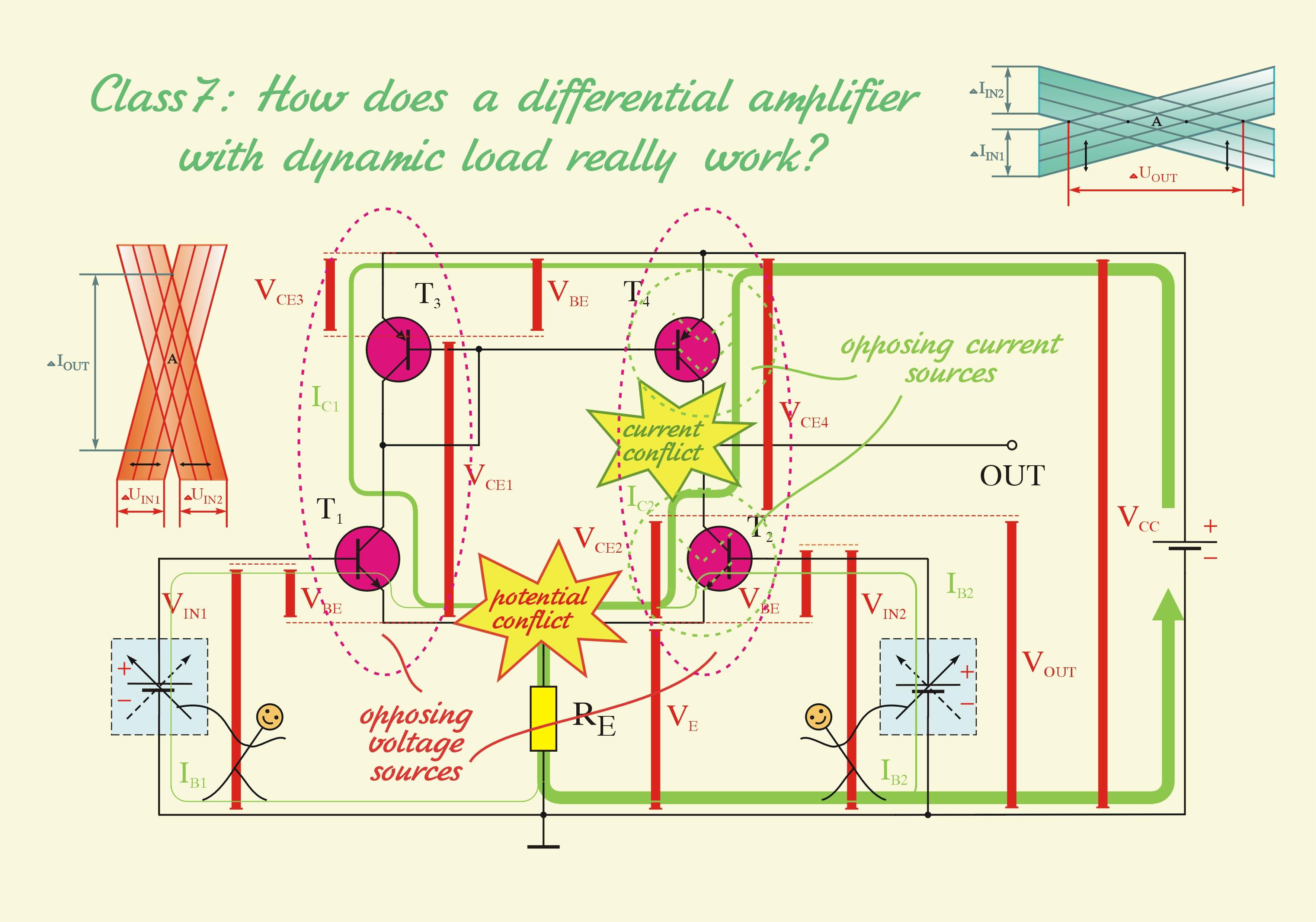
I have drawn the picture and place it in Circuit operation section with the purpose to show a generalized (generic) circuit diagram of a typical ECL circuit. It differs slightly from the particular MECL 10k (the additional reference emitter follower Q4 is omitted and additional resistors are connected in the emitters of the output transistors). I have arranged uniformly the circuit components and stretched the circuit diagram so that it to fill out the drawing. Then, to visualize the invisible electrical attributes, I have overlaid a picture of voltage and current relief. In this attractive presentation, voltages and voltage drops are represented by red colored bars, whose heights are proportional to the corresponding voltage magnitudes (an association with a water column); currents are represented by green colored loops with corresponding topology and thickness that is proportional to the magnitude of the current (an association with a water flow). Having a look at this picture, we can instantly get a notion of how "high" voltages (drops) are and how they are related; we can see how big currents are and how they flow. I have been using this technique since 80's and I have been trying to popularize it... but without any success... just because I was (and still am:) nobody... In 90's, I was drawing a lot of such colorful pictures by using Corel draw editor (see for example our favorite differential amplifier but here with dynamic load). In the early 00's, when I started circuit-fantasia, I was creating a lot of such but animated presentations implementing them as Flash movies (see for example, one "serious" and one funny story that I gave to Tom Hayes). I have been even using on-line presentations where graphical voltage bar (diagram) representations are driven by the very real circuit under investigation (see for example, the story about Ohm's law). It would be very useful if simulating programs had such a graphical output... Finally, when I realized that content is more important than form, I began drawing manually such colorful pictures using only fiber pens with various colors...
I like this picture as it is informative and self-explaining. But if you think it is too ornate, I can redraw it in this manner but retaining only the essential differential part and removing some of the more inessential circuits (the previous stage, the output emitter followers or/and the reference voltage divider). In this case, I can afford to draw another picture for the case of low input voltage (logical "0"). Thus we may describe the two circuit states linking the texts to the two figures. Circuit dreamer (talk) 21:59, 24 October 2009 (UTC)
- It's a very nice picture, but not a style I've ever seen before; is there a source for drawing voltages on schematics this way? Now that I've studied it, I think I understand it well enough -- well enough to spot mistakes like VCE3 anyway.
- Instead of popularizing it, just get it published; then we could use it. Dicklyon (talk) 20:14, 24 October 2009 (UTC)
- If you are teaching a formal class, the students more-or-less have to sit still for the explanation of the diagram, and they benefit by using their new knowledge of the diagram for several circuits. Wikipedia readers might or might not have the patience to figure out the diagram, and if they do, they only get to apply it to one circuit (unless they start drawing their own diagrams in this style). I'm leaning towards saying the diagram is too much of a departure from the usual circuit diagram to ask our readers to learn. --Jc3s5h (talk) 04:08, 25 October 2009 (UTC)

- Dicklyon and Jc3s5h, thank you for your appreciation! I have a compromised solution to the problem that will satisfy both the ordinary and profound Wikipedia readers - to draw three versions of this picture with identical dimensions and then to give an opportunity to the very readers to choose the desired version. The three versions can be:
- Pure circuit diagram (without overlaid voltage bars and current loops)
- Circuit diagram with overlaid voltage bars and current loops at low input voltage (logical "0")
- Circuit diagram with overlaid voltage bars and current loops at high input voltage (logical "1")
- The first picture will be placed in the article and two links inserted in the capture will point to the other two versions (see the exemplary figure on the right). A more sophisticated implementation may be based on dynamic HTML (mouseover effect); but I'm not sure if wiki markup supports this feature. Circuit dreamer (talk) 14:44, 25 October 2009 (UTC)
- Dicklyon and Jc3s5h, thank you for your appreciation! I have a compromised solution to the problem that will satisfy both the ordinary and profound Wikipedia readers - to draw three versions of this picture with identical dimensions and then to give an opportunity to the very readers to choose the desired version. The three versions can be:
- I have a better idea. Just leave off the unconventional voltage bars, and make just two diagrams, which we can put into the article. It's not unusual to show currents on schematics, and to label voltages at nodes; it's just the red stripes and bars that are unique and therefore confusing. Showing the current switching action via a pair of drawings for the two states seems like a good idea. You might want to limit the arrows to just the most important currents, as on the first schematic on this page. Dicklyon (talk) 16:46, 25 October 2009 (UTC)
Summarizing the key points of the discussion
I suggest to begin extracting and summarizing as final conclusions the key points of our discussion upon which we have reached some agreement. After that we may move them to the main article and to other related articles as well. I start the list with the hope that you will enrich it with more wisdom:) Circuit dreamer (talk) 17:56, 26 October 2009 (UTC)
- Digital circuits are actually analog circuits that are made operate as digital ones at the ends of the input range. They operate as analog circuits in the transition area.
- The simplest 1-transistor amplifying stages are inverting as they are implemented by "enhancement mode" transistors (when the input voltage increases, the collector current increases as well) and the voltage drops across their collector-emitter parts are taken as output voltages.
- Logic gates are overdriven DC analog amplifiers without biasing. The transistors of DCTL, RTL, DTL and TTL can stay in three conditions: saturated (at logical "1"), in active regime (during the transition) or cut-off (at logical "0").
- ECL transistors can't operate only in active regime (in both the logical "0" and logical "1" input signal) since, when cascaded, they will amplify the input voltages (the big problem); a DC drift will propagate and accumulate through the consecutively connected stages as well (the smaller problem).
- ECL (input) transistors can stay in two conditions: in active regime (at logical 1 and in transition area) or cut-off (at logical 0). As a result, they change alternatively their condition (...active -> cut-off -> active -> cut-off...) along the chain. The cut-off transistors stop the drift by separating the output voltage from the input voltage; they replace the input voltage by the constant supply voltage (0 V).
- These logic gates consist of two parts: an input part that implements the logical functions and an output part that boosts the weak input part.
- DCTL and ECL have the same logical parts consisting of parallel connected electronic switches (BJT transistors with parallel connected collector-emitter parts). An ECL gate includes a DCTL gate; ECL is an improved version of DCTL in regard to saturation problems.
- To avoid saturation, the current steering idea is used in ECL. It is implemented by a 3-component structure where a current-stable element (or just an ohmic resistor) is conected in series to two connected in parallel (voltage-controlled) voltage-stable elements. This circuit is called by the figurative and self-explaining (in regard to the structure) descriptive name "long-tailed pair".
- In regard to usage, a long-tailed pair is named "differential amplifier", "emitter-coupled amplifier", "analog multiplier", "an amplifier with voltage-controlled gain", etc.
- I disagree or decline to agree in part.
- "As all these logic stages are implemented by "enhancement mode" transistors (by analogy with MOS) and the voltage drops across their collector-emitter parts are taken as outputs, they are inverting."
- I try to explain why all these (common-emitter, common-source and the old common-cathode) stages are inverting. If the transistors could work in some kind of "depletion mode" or if were taken the output in parallel to the collector (drain, anode) resistor, these stages would were non-inverting ones (when the input voltage increases, the output voltage will increase as well). Circuit dreamer (talk) 19:02, 26 October 2009 (UTC)
- The output taken from the collector of the reference transistor is certainly a delayed, non-inverted, and level-shifted copy of the decision-making input. The output of the emitter follower (Y in the colorful schematic) is a delayed and non-inverted copy of the decision-making input. --Jc3s5h (talk) 21:35, 26 October 2009 (UTC)
- I agree with you about ECL. But above I've meant the simplest 1-transistor amplifying stages acting as logic inverters. Circuit dreamer (talk) 23:12, 26 October 2009 (UTC)
- I don't understand what "collector-emitter parts" means and ECL provides both inverting and non-inverting outputs.
- If you prefer, replace with "collector-emitter junction". I mean that only the collectors and the emitters of the input transistors are joined (the bases are not). Circuit dreamer (talk) 19:02, 26 October 2009 (UTC)
- "These logic gates consist of two parts: an input part that implements the logical functions and an output part that boosts the weak input part."
- ECL also performed logic by connecting output nodes together. This was known colloquially as "emitter dotting"[2].
- Maybe, you mean "wired-OR" implemented by connecting the "open emitters". I'm not (still) sure if it is right to attribute this logical function to the basic ECL logic gate. IMO in this case we have a new logic compound gate consisting of separate sub-gates. Circuit dreamer (talk) 19:20, 26 October 2009 (UTC)
- ECL also performed logic by connecting output nodes together. This was known colloquially as "emitter dotting"[2].
- "DCTL and ECL have the same logical parts consisting of BJT transistors with parallel connected collector-emitter parts. An ECL gate includes a DCTL gate; ECL is an improved version of DCTL."
- I don't have enough literature about DCTL to decide if I agree. I suspect ECL preceded DCTL, if so, the statement is incorrect. --Jc3s5h (talk) 18:35, 26 October 2009 (UTC)
- I don't try to say and I don't know what came first (the chicken or the egg:) in this case. I have only said that an ECL gate includes a DCTL one; ECL = DCTL + current steering circuit. In regard to saturation problems, ECL seems to be more perfect than DCTL. Circuit dreamer (talk) 19:28, 26 October 2009 (UTC)
- I don't have enough literature about DCTL to decide if I agree. I suspect ECL preceded DCTL, if so, the statement is incorrect. --Jc3s5h (talk) 18:35, 26 October 2009 (UTC)
- Well, let's compare them. A DCTL logic gate consists of a few parallel connected and grounded transistors having a common collector resistor; it implements NOR function. The input part of an ECL logic gate contains the same components (parallel-connected T1, T2 having a common collector resistor RC1) and it implements the same NOR function. The other elements (T3, RE and R<ssub>C3) prevent saturation by implementing the current steering idea. They also "lift" the emitters of the input transistors above ground to ensure the cut-off. Circuit dreamer (talk) 23:40, 26 October 2009 (UTC)
- In that sense it "contains" lots of other things, too, like differential amplifier, inverter, and such. But the existence of transistors in parallel to do logic, without base resistors, is not enough to call it DCTL, which is a family that has grounded emitters and which saturates; the ECL gate does not "contain" these characteristics. I have no problem describing it in terms of DCTL or differential amplifier, long-tail pair, or whatever you can back up with sources; but without sources, no. Dicklyon (talk) 00:41, 27 October 2009 (UTC)
I also "disagree or decline to agree in part". I think this is a summary of how Circuit-Dreamer likes to teach this material, not a summary of any discussion here. Many of these points are idiosyncratic, or I will believe they are until I see sources that support them. I don't think this article needs to resort to a tutorial approach with such generalities as "there are only analog circuits;" if the digital states are first described, as we describe the behavior as digital, then analog effects can be brought into a subsequent discussion of performance. But whichever way we do it, we should build it as much as possible from what sources say, not from an original idiosyncratic tutorial approach. Dicklyon (talk) 19:34, 26 October 2009 (UTC)
- Well, let me then summarize only my insights... Maybe, we will benefit something from them... Circuit dreamer (talk) 19:46, 26 October 2009 (UTC)
- I won't say anything about Circuit-dreamer's electronic views, since I'm sure anything I say will be misinterpreted. If Circuit-dreamer wants to promote his way of "looking at" electronics on Wikipedia, nothing can stop him. On the other hand some of the "sources" I see being used to support material on Wikipedia pages are just as shaky. This latter problem stems from the practice of googling instead of actual research in authoritative sources. When the subject matter is not well understood by the writer a google search will usually bring up a sub-par reference that is then misinterpreted, resulting in a loosely connected assemblage of unreliable factoids. A better approach is to learn the subject matter first, develop a plan for the page, and then write the page. Important claims that are not obvious should be supported by citations in authoritative sources. Earlier I presented a rough outline for this page. You don't need to be a rocket scientist to understand ECL circuits and basic transistor electronics. So instead of all this discussion about specifics why not decide on an overall plan for this page. Then, as it starts to come together those details that need citations can be researched. Zen-in (talk) 06:53, 27 October 2009 (UTC)
Revealing the truth about ECL circuits
(seeing the forest for the trees)
I am in the seventh heaven as I have finally revealed the fundamental idea of ECL... It is not differential amplifier (more precisely, emitter-coupled amplifier) or current steering although, in the middle of transition, the circuit is exactly a differential amplifier (an emitter-coupled amplifier) that steers the current between the legs. Well, I agree it steers; but imagine some curious and profound visitor like our anonymous 60.241.12.136 (see DC drift of output section above) browses through this highest Google ranked page in the hope of grasping the basic ECL idea. Reading "current steering" he/she will want to know why the emitter current is steered between the two legs; with what purpose is the current steered? Why a differential amplifier is used? What problem does it solve here? To answer these questions, we have first to show what the fundamental problem of ordinary logic circuits is and then to show how this problem is solved in ECL. I can say (and will say at the end) in a few words what this genius idea is but let me first expose it in detail as it deserves more respect. Circuit dreamer (talk) 07:47, 3 November 2009 (UTC)
The problem of saturation
Differential amplifier, emitter-coupled amplifier and current steering are misleading concepts here. They cannot explain what fundamental problem ECL has solved as they focus our attention to the middle part of transition where actually there is no any problem! In this area, the transistors of all the ordinary logic circuits (RTL, DCTL, DTL and TTL) work perfect as common-emitter stages in active regime. If we were staying in this area, there was no any need to replace them with this more sophisticated and odd 3-component structure figuratively named long-tailed pair as it would do the same - it would work as the same common-emitter stage!
A problem appears when the input voltage approaches the high threshold (logical "1") and the transistors of the ordinary logic circuits (RTL, DCTL, DTL and TTL) saturate; as a result, they work slowly. But, as our curious reader would think, the differential (emitter-coupled) amplifier couldn't solve this problem as, in this area, the reference transistor T3 is cut-off and the differential amplifier is not an amplifier. That's why, to realize what happened above, the reader has created his own "philosophy" about ECL thinking of a differential amplifier not as of an amplifier but as of a comparator. Really, the long-tailed pair is cut in two and this structure is no more a differential amplifier; its two new parts are something else. So, the paradox of this classic viewpoint is that we use a differential amplifier where actually it is not a differential amplifier!
Saturation is the fundamental problem that ECL circuits solve at high input voltage (logical "1"). This and only this is the amazing feature of ECL; the other advantages (as the presence of two inverse outputs) are inessential. So, it is our primary duty to show in this page the basic idea (the clever trick, the circuit solution, the remedy...) that is used to prevent saturation. But how can we prevent saturation? Let's see and compare various anti-saturation techniques.
How to prevent saturation:
We can drive the transistor from the side of the base and from the side of the emitter. So, we may prevent saturation indirectly from the side of the base by limiting the base current or directly from the side of the emitter by limiting the very collector current.
...from the side of the base...
We have two techniques for limiting the base current that require the presence of a base resistor (i.e., they are inappropriate for direct-coupled circuits).
- The simplest and obvious solution is to decrease the base current by increasing the base resistance or by connecting an additional resistor between the base and ground (forming a voltage divider). But the large tolerances of β make this approach unrealizable [3] as the collector current and the point of saturation will depend on the particular transistor.
- Another but reliable and wide used β-independent technique for preventing saturation is to detract the excessive base current by a diode negative feedback (connecting a Schottky diode between the collector and the base). Until the transistor is in active mode, the diode is cut-off and does not affect the base current. When the transistor approaches the saturation point, the diode turns on and deprives the excessive base current.
...from the side of the emitter
Finally, we may try to avoid saturation by limiting the very collector (emitter) current and thus we will finally arrive at ECL. But we cannot set the desired emitter current in a common-emitter stage (DCTL) simply by inserting a constant current source (or, in the simpler case, an ohmic resistor) between the emitter and ground as we will not be able to control at all (or slightly, in the case of the resistor) the collector current from the base. Why? The answer is that the current source (the emitter resistor) will introduce series negative feedback and the common-emitter amplifying stage will transmute into a stage with emitter degeneration. As a result, when we change the input base voltage to change the collector current, the transistor changes in the same manner its emitter voltage and we do... nothing:( Figuratively speaking, when we "move" the base voltage, the transistor "moves" in the same manner its emitter voltage (it operates as an emitter follower). The emitter voltage has become "soft", "pliable", "movable"...; but to control the collector current the emitter voltage has to be "hard", steady, fixed...
This is a fundamental problem of analog circuit design - how to set the desired collector current (the quiescent point) from the emitter without losing control from the base. Or, in other words, how to make the emitter voltage "soft" for the undesired influences and "hard" for the useful input voltage applied to the base. Typical examples: an AC amplifier with emitter degeneration suppresses the slow DC variations and amplifies rapidly changing AC input variations; a differential transistor amplifier suppresses common-mode signals and amplifies differential input signals; finally, an ECL gate suppresses the input voltage variations near to the high threshold (input logical "1") and amplifies them significantly during the transition. It is clear that there is some common powerful idea in these apparently different circuits... What is it?
Obviously, to make the emitter voltage "soft", we have to insert a constant current source (actully, a current-stable element) and v.v., to make the emitter voltage "hard", we have to insert a constant voltage source (a voltage-stable element). Instead to replace the current source with a voltage source we may just connect the voltage source in parallel to the current source as it will define the voltage across the combination of two elements. In the first two examples above, the voltage sources are permanently connected to the current ones but they appear only at useful input signals. In the AC amplifier, the bypass emitter capacitor follows the slow DC variations and does not affect the current source; but it begins acting as a constant voltage source at rapidly changing AC input variations. In the differential amplifier, the right emitter voltage follows the left one at common-mode and does not affect the current source; but it becomes steady (or opposite changing) at single-ended (or differential) mode. In ECL gate, solely the constant current source is connected in the emitter when the input voltage is near to the high threshold (input logical "1"); both the constant current source and the constant voltage source are connected in the emitter during the transition (the sources are commutated by the transistor's base-emitter "diode switches" S1 and S2 on the picture). Let's consider the three possible configurations.
VIN < VL, VIN = VL (logical "0"). T1 is cut off; VY = 0 V and does not depend on VIN. Both the current source (RE) and the voltage source (T3) are disconnected from the input part (but they are connected to each other).
VL < VIN < VH (transition). T1 operates in active regime (common-emitter configuration) with both the parallel connected current source (RE) and voltage source (T3) inserted in its emitter. There is no negative feedback. VY depends significantly on VIN since the voltage source dominates over the current one and fixes T1's emitter voltage (it is "hard").
VIN = VH, VIN > VH (logical "1"). T3 is cut off and there is no voltage source. Only the current source (RE) is connected in T1's emitter (emitter degeneration). There is a series negative feeddback. VY = VL and does not depend at all (in the case of constant current source) or depends slightly (in the case of emitter resistor) on VIN since T1's emitter voltage is "soft".
Finally, let's say the simple truth about ECL with one sentence:
ECL is based on a transistor stage with switchable voltage and current emitter sources: at low input voltage, the sources are disconnected from the emitter; during the transition, both the voltage and current source are connected; at high input voltage, only the current source is connected to the emitter.
Circuit dreamer (talk) 20:35, 2 November 2009 (UTC)
Side comment
Hi CD. I'm not too involved in this article, so I won't get into the whole discussion. I just wanted to remind you to keep your talk page posts brief and concise so you don't overwhelm everyone else. Also, this isn't really the place for draft versions of an article. -Roger (talk) 17:19, 6 November 2009 (UTC)
- Roger, thank you for the gentle reminder. The problem is that ECL circuits (like negative resistance circuits) are poorly and inconsistently explained in sources. We, wikipedians, have not to convey blindly what reputable sources say (just because they are reputable); we have to process sensibly the existing knowledge; we have to be smart mediators. For this purpose, you should admit, the very we have first to realize what the fundamental idea of ECL circuits is and how they operate and only then to create the main article. The opposite is just an absurd (imagine a teacher/translator that does not understand but explains/translates the subject:) Saying "understanding" I mean discerning well-known simpler circuit building blocks and circuit phenomena in the discussed circuit (ECL here). This is my mission here. I won't move all my insertions from the talk page to the main article; do not think of them as of a draft version. I am ready even to remove them if they are disproved. Circuit dreamer (talk) 19:21, 6 November 2009 (UTC)
- Dicklyon, understanding is the most important for me. Once I realized what the fundamental idea is and how it is implemented in the particular circuit, I haven't any problems. About my intentions: I will begin extracting the key points from the written above and will move them into the article if they are confirmed (to some reasonable extent) by the reputable sources below. Circuit dreamer (talk) 22:16, 7 November 2009 (UTC)
Sources for improving the article
Let's start a collection of sources about how ECL works, and use them to improve the article:
Reliable sources (book, published papers, etc.)
- Forrest M. Mims (2000). The Forrest Mims Circuit Scrapbook, Volume 2. Newnes. p. 115. ISBN 9781878707482.
In operation, input transistors ... form a differential amplifier.
- Sajjan G. Shiva (1998). Introduction to Logic Design (2nd ed.). CRC Press. p. 517. ISBN 9780824700829.
...the current steering mode of operation...
- Taub, Herbert; Schilling, Donald (1977). Digital Integrated Electronics. McGraw-Hill. p. 229–256.
- William R. Blood Jr. (year=1988/1980). MECL System Design Handbook (PDF) (4th ed.). Motorola Semiconductor Products, republished by On Semiconductor.
{{cite book}}: Check date values in:|year=(help); Missing pipe in:|year=(help)
- Fundamental Digital Electronics by Brian Lawless, Unit4: ECL Emitter Coupled Logic (excellent)
- Modern digital electronics By R P Jain (page 111)
- Electronic Materials Handbook: Packaging (page 163) by Merrill L. Minges, ASM International. Handbook Committee
- Stretch Circuit Memo #3 by Yourke (maybe, we should decipher the original Yourke's material?)
- Most are poor sources, Mims especially. If you just want to enumerate a list of random facts about ECL, with verifiable citations, you have all you need. But that results in a very dry article with no useful purpose. Maybe we should bring back CD's colorful illustrations with the stick men. At least they made things interesting. Zen-in (talk) 21:38, 7 November 2009 (UTC)
- BTW his circuit diagrams are handwritten:) but they are not colorful:( Well, I second your opinion about this source. Maybe, Dicklyon should at least move it downwards. Circuit dreamer (talk) 21:56, 7 November 2009 (UTC)
Other stuff of unknown provenance
- Emitter-coupled circuits (profound written)
- Halbleiter-Schaltungstechnik (in German)
Why the input resistance is low during the transition
(a reply to the "citation needed" note in the lede)
During the transition the ECL gate behaves as an ordinary emitter-coupled amplifier in active mode that is described comprehensively in electronics textbooks. The emitter voltage of the input transistor is fixed by the reference transistor and changes slightly. So, there is no negative feedback (emitter degeneration) and the input transistor operates in a common-emitter mode. The input resistance is low and it is determined by the the base-emitter junction resistance. Circuit dreamer (talk) 13:08, 15 November 2009 (UTC)
- Nonsense; the input impedance will be on the order of thermal voltage divided by bias current, somewhat reduced by negative feedback from the emitter. It will usually be set to a considerably higher impedance than the output impedance that you're calling low, no? And where's the source for this? My estimate says the input impedance at mid-level is not less that it is at high level, but I'm not going to put my analysis into the article without a source. Dicklyon (talk) 05:14, 17 November 2009 (UTC)
- We are talking about small-signal resistance, aren't we? Let's consider the input resistance at the three ECL states:
- Input logical "0". From the point of view of the previous stage, there is no circuit (load) connected at this state since T1's base-emitter voltage is less than the cut-in voltage and the base-emitter junction is cut-off. So, the input resistance (looking into T1's base) is extremely high and the previous stage does not "see" anything.
- Transition. Now, the previous stage "sees" a common-emitter stage (T1 with fixed emitter voltage). The input resistance is low - 2rBE (Tietze & Schenk's Halbleiter-schaltungstechik).
- Input logical "1". Finally, the previous stage "sees" a common-collector stage or emitter follower (T1 with "moving" emitter voltage). The input resistance is high enough - (1 + β).RE. In the case of emitter current source connected, it is infinite; the previous stage does not "see" anything as above (at input logical "0") and the base current does not change at all when the input voltage wiggles since the collector current is steady.
- As a conclusion, during the transition "0" --> middle --> "1", the circuit changes its input resistance three times in sequence: infinite --> low --> high. The low input resistance during the transition shunts the stray capacitance; so, the circuit should be faster because of that. It is interesting to compare ECL with DCTL (I continue asserting they are related): an ECL circuit is low-resistive only during the transition (when it is needed) while a DCTL circuit is low-resistive both during the transisiton and at logical "1". Circuit dreamer (talk) 16:15, 17 November 2009 (UTC)
- Like I said, your argument is flawed, and essentially useless without a source to back it up. I agree that it goes from very high impedance when low to pretty high when high, and maybe somewhat lower in the middle; but you're wrong on two counts: (1) the emitter voltage is not fixed when the amplifier is near the balanced state; it moves about half as much as the input voltage, so there's some degeneration; (2) the relevant dynamic resistance of the junction is determined by the exponential I–V relationship, and is about 26 mV divided by the emitter current, times beta, which at low bias current can be fairly high, much higher than the 50 ohms or so that you call "low" at the output; for example, at 3 mA bias current, or 1.5 mA in one leg at balance, and beta of 50, it's about 900 ohms, but then double that due to the emitter moving half way, so about 1800 ohm. I suppose that's what you're calling 2rBE, but calling that "low" is not appropriate, compared to the impedance of the outputs and wires. Having it shunting the input capacitance is irrelevant. At least, that's the way I figure it. Without a source, nothing needs to be said about all this. Dicklyon (talk) 19:48, 17 November 2009 (UTC)
- But it is right for differential ECL where the emitter voltage is really fixed, isn't it? Circuit dreamer (talk) 21:36, 17 November 2009 (UTC)
About "overdriven differential amplifier"
I have used the term "overdriven" in the lede to encompass the three states of an ECL gate: logical "0" (the input transistor is cut-off, the reference one is in active mode); transition (the two transistors are in active mode) and logical "1" (the input transistor is in active mode, the reference one is cut-off). So, "overdriven" means "driven with high enough input voltage so that one of the two transistors to be cut-off". We can also say that the differential amplifier is saturated at the ends but this term is controversial. Circuit dreamer (talk) 15:25, 15 November 2009 (UTC)
- Over driven (two words) implies driving a transistor stage into saturation. Driven into cut-off may be the term you want to use. ECL signals are not high level, so "driven with high enough input voltage..." doesn't apply here. Zen-in (talk) 18:16, 15 November 2009 (UTC)
- Zen-in, Google and dictionaries suggest "overdriven". I want to encompass the three states ("0", transition and "1") by one word (distorted?). Maybe you are right about "high enough voltage"; I mean a voltage magnitude in regard to the reference voltage (-1.3 V) that is sufficient to saturate (+0.4 V) or to drive into cut-off (-0.4 V) the transistors. In regard to VEE = -5.2 V these magnitudes are +3.5 V (logical "0") and +4.3 V (logical "1"). Circuit dreamer (talk) 18:30, 15 November 2009 (UTC)
- I've realized what the problem is. Note the emitters are "lifted" in regard to VEE by +3.2 V. So, if "over driven implies driving a transistor stage into saturation", we may use it here since we may think of an ECL gate as of a bipolar circuit with virtual ground of -1.3 V (a bipolar circuit may be saturated in both the polarities). Then, we may "overdrive" it by positive input voltage of +0.4 V (-0.9 V in regard to real ground) and by a negative input voltage of -0.4 V (-1.7 V in regard to real ground). Circuit dreamer (talk) 18:57, 15 November 2009 (UTC)
- Right; it's one word. But when you are talking about a transistor circuit being overdriven it means the base current is large enough to saturate the transistor. Of course the current mode logic that is the basis for ecl does not saturate. I think you are thinking of your over helper stick men. Zen-in (talk) 08:04, 16 November 2009 (UTC)
- You've discussed a similar problem (about the meaning of "saturation") with Dicklyon above. I remember, it was in 80's, I had written in an article that the op-amp was "saturated" (I had meant that it had reached the positive or the negative supply rail). The professor writing an opinion said to me that it was wrong as an op-amp couldn't saturate because its output transistors (emitter followers) couldn't saturate. Then I said him that I had used the word "saturation" in the broad sense. Similarly, I've used here the word "overdriven" (as Dicklyon have used "saturation" above) in the broad sense to represent both the states where the emitter-coupled amplifier has saturated (in the broad sense) and output voltages have stopped changing (the one - because the transistor is cut-off; the other - because a current source has "appeared" in its emitter).
- The confusion with "saturation" in ECL is bigger than in op-amp circuits since here we say "the ECL is saturated" when the one transistor is in active mode and the other is even cut-off. Maybe clipping is another word for designation this output condition. As I can see from the lede of this Wikipedia page, they have used "overdriven" to designate an excessive input voltage that makes the amplifier "clip".
- You are right sayng "Of course the current mode logic that is the basis for ecl does not saturate". Yes, it does not saturate in the narrow sense of the word (i.e., there are not saturated transistors in the circuit). But it "saturates" (clips) in the broad sense of the word. Circuit dreamer (talk) 16:09, 16 November 2009 (UTC)
- That is ambiguous. How does the reader know what "sense" of the word you mean? If you say it doesn't saturate in one place in the article and then say it does somewhere else you are contradicting yourself. BTW clipping is associated with saturation. One possible solution to your problem is to cite references that use this terminology. But the problem is with "excessive input voltage that makes the amplifier.." There is no excessive input voltage in ecl circuits and collector current is a function of the base current. Zen-in (talk) 17:20, 16 November 2009 (UTC)
"There are single-ended (input) ECL gates based on emitter-coupled amplifier and differential ECL gates based on differential amplifier." Don't all ecl gates have a current mode logic (CML called differential amplifier by some) stage? I think we have already established that ecl gates with single-ended inputs have a CML stage. Motorola's ECLPS Data book shows a few differential input devices, like the MC10E404 Quad Differential AND/NAND gates. The only transistor equivalent circuit is similar to the 10k schematic in the article. Zen-in (talk) 02:38, 17 November 2009 (UTC)
- I took that out; I have no idea what its point was, and there was no source where I could look it up to clarify. Dicklyon (talk) 05:05, 17 November 2009 (UTC)
- As to "overdriven BJT differential amplifier", that seems clear and correct. It's not ambiguous; if we wanted to say the BJTs were overdriven, it would need to be "overdriven-BJT differential amplifier", but that's not what it says. Here is a source that uses terminology like this, but not about ECL specifically. Dicklyon (talk) 05:05, 17 November 2009 (UTC)
Variations of ECL exist that use differential signals; there are actually two wires carrying complimentary versions of the signal from one logic block to another. IBM called it "differential current switch" and used it on the Enterprise System/9000 models 190, 210, 260, 320, 440 and 480. Here is a schematic of one of the circuits:

This was described in E. B. Eichelberger & S.E. Bello, (May 1991), Differential Current Switch—High performance at low power, IBM Journal of Research and Development, V. 35 No. 3, pp. 313–320.
- No, but a customary single-ended ECL circuit was available on the same chip by personalizing the first layer of metal, so they had to be sure to distinguish it from the ECL that was intermingled with the DCS. These were semi-custom gate array chips--Jc3s5h (talk) 07:14, 17 November 2009 (UTC)
When a BJT is overdriven much more current is supplied to the base than is needed to simply turn it on. This result in slower turn-on and turn-off because of the extra time needed to transfer charge to and from the space charge layer. ECL is purposefully designed to minimize these delays. So the word overdriven does not apply to ecl circuits. In your reference the author is not talking about ecl circuits when he uses the word overdriven. This is an example of blind "fishing" for citations using specific text and then using whatever comes up, regardless of its suitability. I just did a google search to prove the theory that An American Cousin killed Abraham Lincoln [4]. But I'm not going to use this reference for obvious reasons. Zen-in (talk) 02:38, 18 November 2009 (UTC)
- When a differential pair (emitter-coupled pair) is overdriven, all the bias current goes through one leg, but neither transistor is overdriven; the amplifier output is at its saturation level, but the transistors are not in saturation. Do you have better words to say that? I already acknowledged that the source I found was not about ECL per se, but it is about an "emitter-coupled clipper" based on an "overdriven differential amplifier", which is the exact circuit and mode of operation that is used in an ECL gate. Dicklyon (talk) 07:50, 18 November 2009 (UTC)
- That is all explained using the current steering wording. The ecl CML stage is designed to have a very small linear region. The transistors have very high current gain and the circuit operates with small input voltage swings (low drive). So the statement in that reference concerning a differential amplifier does not apply to ecl. Zen-in (talk) 16:10, 18 November 2009 (UTC)
A mistake in the figure about Yorke's current switch
The outputs of the p-n-p Yourke's current switch represent logical OR (F+C) and NOR (F+C), not AND (F.C) and NAND (F.C) as it is shown on the figure. Maybe the author of the figure is misled by the very Yourke's original material where he has written F.C instead just F+C according to De Morgan's laws. Circuit dreamer (talk) 21:03, 24 November 2009 (UTC)
- The figure is correct in two senses. First, it is an accurate redrawing of page 608 figure 4 in the cited journal article by Rymaszewski, Walsh, & Leehan. Also, I am convinced the drawing is correct, provided you are using positive logic; that is, logical 1 is a higher voltage than logical 0. If any pnp input is in the low state, the magnitude of the voltage across the emitter-base junction is greater, and the transistor goes into the active region. If any pnp input transistor is in the active region, the node labeled F•C will be more positive than its other state, that is, logic 1. If you write out a truth table, you will see it is the NAND function. --Jc3s5h (talk) 22:47, 24 November 2009 (UTC)
- You are right. Really, the problem was that I was thinking in terms of negative logic. Sorry, it's my mistake. Circuit dreamer (talk) 06:44, 25 November 2009 (UTC)
the gain is high why?
Circuit dreamer, in this edit, I took out the reason you had put for high gain in "As the input stage is loaded with the small T3 input emitter resistance, there is no negative feedback or it is slight enough; as a result, the gain is high and the circuit switches quickly." I don't see a way to interpret what you mean by "the input stage is loaded with the small T3 input emitter resistance". Well, maybe I do; you're looking at T3 as a follower presenting a low-impedance looking into its emitter as a load to the emitter of T1. That seems like a roundabout way to say that a differential pair has a high gain when in its active (non-saturated or non-overdriven) region. Is there a precedent in sources for such description, or is it just something you made up? Dicklyon (talk) 07:39, 14 December 2009 (UTC)
- Dicklyon, as I can see (looking at your previous remarks), we have different notions of this arrangement but we have finally to reach consensus on this stuff as it is a fundamental concept in analog circuitry. Actually, this topic is most typical for a differential amplifier; so we may use the results from this discussion there to explain how a DA operates in a differential and common mode. Now, I will first expose (again) my viewpoint at the topic and then I will search for sources seconding it.
- We have exactly the same two situations for both the arrangements (ECL and DA):
- A common-emitter amplifying stage with a resistor (emitter degeneration) or a constant current source inserted in the emitter. In ECL, this situation occurs in the input stage at high input voltage (logical "1") since the reference transistor is disconnected from the input one and does not affect it. In a differential amplifier, the same situation occurs when the second input voltage follows the first one (common-mode input voltage) and the second transistor does not affect the input one (actually, it does not exist for the input one; this is the famous "bootstrapping" phenomenon). In terms of resistance, here we have high resistance connected in the emitter. Because of the series negative feedback introduced by the high-resistive emitter element, the emitter voltage follows the input one and the gain is less than the gain of the same stage with grounded emitter (in the case of CCS inserted the gain is zero and this is the clever trick to suppress the common-mode input voltage in DAs).
- A common-emitter amplifying stage with grounded emitter or a constant voltage source inserted in the emitter. In ECL, this situation occurs in the input stage during the transition since the reference transistor acts as a kind of (almost) constant voltage source. Yes, I agree, it (an emitter follower with a constant input voltage) is not absolutely perfect but it is still a voltage source. In a differential amplifier, the same situation occurs when the second input voltage is fixed or it changes with the same rate but in an opposite direction (differential input voltage). In terms of resistance, here we have low resistance connected in the emitter. In this case, there is a slight negative feedback introduced by the small resistance connected in the emitter (in the last case, there isn't any negative feedback at all). As a result, the emitter voltage follows slightly the input one and the gain is higher than the gain of the same stage with emitter degeneration (in the case of differential input voltage, the gain should be the same as the gain of the common-emitter stage with grounded emitter).
- So, the ECL circuit has different gains during the transition and at high input voltage; it changes its gain dynamically thus behaving as a nonlinear circuit. Saying "during the transition, the gain is high", I actually mean "during the transition, the gain is higher than the gain at high input voltage". Circuit dreamer (talk) 17:54, 14 December 2009 (UTC)
- Circuit dreamer's explanations are more-or-less applicable when the input changes slowly. However, it would require considerable analysis to decide if a common emitter amplifier with grounded emitter behaves the same (in the active region) as a differential amplifier when the input changes rapidly. Such analysis would be original research, so if the analysis were conducted by an editor (rather than found in a reliable source) it couldn't be included in the article. Simply putting a qualification in the article wouldn't do, because in practice, the input often does change rapidly. --Jc3s5h (talk) 21:42, 14 December 2009 (UTC)
- True, when the gain is high, it would be unusual for the input to be so slow that the output slope would be higher by the gain factor; in that sense, the gain is higher than needed, and behavior is dominated by the dynamics. My point, and yours too, I think, is that explanations in wikipedia should follow explanations in reliable sources. Otherwise, Circuit dreamer would have license to ramble on at length about his view of how it all works. I'm not saying his view is wrong, just that it's out of place in wikipedia if not backed up by a reliable source. Personally, I am not familiar with describing the behavior of a differential pair in terms of one transistor with a variable emitter degeneration; it seems like a roundabout approach, and I think we don't need it; if it can be shown in sources, I'll reconsider. Dicklyon (talk) 22:26, 14 December 2009 (UTC)
History
Are ecl circuits in production, or aren't they made anymore?
If ecl isn't in production, that could be added in the history section of the article. —Preceding unsigned comment added by 94.213.108.115 (talk) 00:27, 1 September 2010 (UTC)
- ECL is produced by ON Semiconductor, for example. Prari (talk) 00:06, 2 September 2010 (UTC)
Comments and additions
I think this is truly a great article. However, it is not clear in a few passages and it fails to deliver some important information I think should be included in it.
1. "In some cases 50Ω line termination resistors connected between the bases of the input transistors and −2 V act as emitter resistors." It's not clear where that "-2V" is coming from and what it means.
2. I believe it would be important to list the maximum and minimum input voltages for ECL circuits which are usually between -0.9V and -0.75V for high and between -1.75V and -1.6V for low. It should also be pointed out that transistors should all be matched with VBE=0.75V. Although it is clear by looking at the circuits, the article should also say that ECL circuits provide OR and NOR functions.
ICE77 (talk) 21:58, 15 February 2011 (UTC)
- In some cases a separate power supply of -2 V is provided for terminating the emitter follower pull-down resistors. When the resistor value is 50 Ω the resistor is likely to be located at the input of the circuit that is receiving the signal, and the distance between the transmitting an receiving circuits is likely to be long enough that the connection must be treated as a transmission line. Jc3s5h (talk) 01:49, 16 February 2011 (UTC)
Let's add to the article then. A reader can't guess it.
ICE77 (talk) 02:15, 16 February 2011 (UTC)
Dubious?
Glrx has made a number of changes, including labeling the following statement dubious:
ECL circuits in the mid-1960s through the 1990s consisted of a differential amplifier input stage to perform logic, followed by an emitter follower to drive outputs and shift the output voltages so they will be compatible with the inputs.
The explanation for this label seems to be the following HTML comment:
With the advent of integrated circuits, the collector to base voltage in the differential pair could be reduced, and the output level shifting need only be a junction drop. An emitter follower could then perform as both a level shifter and an amplifier.
I fail to see what is dubious about this statement, or how there is any contradiction between the visible statement in the article compared to the HTML comment. Jc3s5h (talk) 16:24, 17 August 2012 (UTC)
- The issue is discrete versus integrated circuit implementations. Where is the source that says discrete ECL disappeared in mid 1960s?
- The statement is probably false for discrete ECL. Discrete versions of ECL need a large VCB to keep them fast, so they alternate NPN/PNP stages or use zener diode level shifters. IBM Standard Modular System (SMS) included discrete ECL; SMS was "in use with legacy systems through the 1970s" (an editor claimed ECL was used in the IBM 1401); also SMS saw continued use in S/360 peripherals (i.e., peripherals in mid 1960s, but not clear if any peripheral used ECL).
- The tagged statement is probably true for monolithic IC technology because only one flavor of transistor was usually available/fast. Statement certainly true for Motorola MECL and IBM's Monolithic Systems Technology (MST).
- The statement need not be true for hybrid circuits, but it looks like IBM SLT hybrids used only NPN transistors.
- Also, why did ECL stop using emitter followers after the 1990s? That other logic technologies took over doesn't kill the utility of the emitter follower in ECL.
- My intent is to reshape the dubious statement to be monolithic ECL used an emitter follower as a level shifter. My sense is that SSI ECL works because the differential stage can be fast and fragile but slightly degraded; the output emitter follower and wire delay may obviate need for ultimate speed; power consumption/package dissipation is an issue so small VEE important. But I have no source.
- Glrx (talk) 18:11, 17 August 2012 (UTC)
- I agree the statement should be limited to monolithic ECL; there are probably discrete cases but I don't know if they are worth mentioning. I think the statement about the 1990s is on account of ECL falling out of use by the late 1990s. It would be challenging to locate the remaining niche applications and determine if the statement was still true for these applications. Jc3s5h (talk) 19:01, 17 August 2012 (UTC)
Was ECL only implemented in silicon - or was GaAs also used ?
or any other semiconductors ? - Rod57 (talk) 05:29, 3 January 2016 (UTC)
- Maybe Silicon-germanium Heterojunction Bipolar Transistors? And many books contrast GaAs (FET) with ECL (bipolar) logic. Dicklyon (talk) 05:38, 3 January 2016 (UTC)
- Thanks. If I read that right ECL can use either Si BJT or SiGe HBT. It would be good to add that to the article and say which came first and compare them and say if any other transistor types were used in ECL. I'll add something based on your source and maybe it will get extended. - Rod57 (talk) 09:02, 3 January 2016 (UTC)
- OK - I added
ECL often uses Si BJTs but can also be built with faster SiGe HBTs.[n] - Can we say what types of bipolar transistors would be suitable or unsuitable for ECL ? And can someone say which has been used for discrete ECL and LSI-ECL ? - Rod57 (talk) 09:21, 3 January 2016 (UTC)
- I'm tempted to revert the addition because the source is confusing and the result is not clear. That SiGe HBT could be used does not imply that it is commonly used in ECL logic. I vaguely remember a company pushing fast (ps) ECL logic, but I think that was before HBT, and I don't think it took off. ECL as a commodity wasn't an attractive market. If you were doing big logic, then you cooked your own chips and invested in exotic ways to cool them.
- I'm unfamiliar with BiCMOS, but the schematics I googled do not use ECL differential pair topology (but see below). A process guy who loved ECL and IBM said the winning feature was the bipolar transistor's high transconductance; FETs don't even come close. A different process guy said the magic of the BiCMOS hybrid was doing all the on chip logic with low-power high-speed CMOS and then using the big gun bipolars to drive signals off the chip and into the cold, cruel, current-hungry outside world. You didn't need high currents or high gain for the low-capacitance CMOS on-chip logic.
- The insertion's cited source mentions that HBT ECL is used in some logic for communications circuits, but that does not imply that HBT has a significant presence in ECL logic ("ECL often uses Si BJTs but can also be built with faster SiGe HBTs" has a weasel-word aspect). Communications circuits are a narrow niche. Communications circuits often use SiGe HBT devices to gain amplifier performance in microwave monolithic integrated circuits. If the process is used already, then building some high-speed logic (such as a high-speed prescaler for a PLL communication circuit) could make sense. That doesn't mean that those communications companies are providing ALUs or barrel shifters or significant amounts of ECL logic. They play the same game that was played twenty years ago: use a fast Motorola ECL IC prescaler to divide the VCO and drive a slow Motorola CMOS PLL chip. With BiCMOS it can be built on one chip instead of two.
- I don't think we need to raise the issue about SiGe HBT ECL, but if we do, then it should follow the source. For the given source, the statement should be limited to SiGe HBT ECL is used in communications circuits.
- To approach it differently, if somebody like IBM is building its computers out of SiGe HBT ECL, then it should be easy to find references that say that. WP:DUE. I don't know what IBM is using for its logic.
- There does seem to be substantial laboratory work for SiGe HBT ECL, but I'm not turning up anything that says it is common.[5] BTW, page 570 of that book states that BiCMOS chips could make use of ECL logic, but the statement sounds speculative. The book states that CMOS memories with ECL peripheral drivers have been made, but that's not really using ECL logic. The page goes on to state that the significant applications have been in mixed signal situations such as a 10 GHz SiGe BiCMOS frequency synthesizer using 17 mW.
- Glrx (talk) 21:39, 3 January 2016 (UTC)
- Other than the Stretch and a few 360 parts, I don't find evidence of discrete ECL. And I agree the HBT GeSi stuff is probably a red herring, not real. Dicklyon (talk) 22:26, 3 January 2016 (UTC)
- Thanks everyone for the input. We could extend the insert to say "as rarely used in communications circuits" ? but is ECL for communications really ECL or is it PECL or current mode logic ?
- I originally just wanted to confirm only silicon was used and perhaps explain why GaAs was never used to improve the speed. (GaAs defect density prevented scale down ?)
- Even if a use is not common it, IMO, should still be mentioned (eg as 'rare' or 'occasional').
- It would be great if the History section could mention that Stretch and a few 360 parts used discrete ECL (but I'm out of time to find a source). - Rod57 (talk) 14:30, 4 January 2016 (UTC)
- The first paragraph of the history section already mentions the use of current steering logic in 1956; obviously discretes were used in 1956. Perhaps the history section should have a sentence put in to indicate the first use of hybrid integrated circuits, and the first use of monolithic integrated circuits to implement ECL.
- I worked at IBM at the time the last few generations of ECL mainframes were being designed, and the first CMOS top-of-the-line mainframes were introduced. HJTs were under investigation at that time for other uses, but the considerations for mainframe logic were cooling and circuit density. ECL is high power and occupies more area on the chip, for the same function, compared to CMOS. Also, operating systems and software were getting better at distributing work among many processors, so substituting a larger number of CMOS CPUs for a few ECL CPUs was becoming more effective. GaAs defect density was not a topic of conversation. Jc3s5h (talk) 16:17, 4 January 2016 (UTC)
- Other than the Stretch and a few 360 parts, I don't find evidence of discrete ECL. And I agree the HBT GeSi stuff is probably a red herring, not real. Dicklyon (talk) 22:26, 3 January 2016 (UTC)
What can we say about the transistors used at various times in the evolution of ECL (as used for CPU logic)
Only once (in the intro/lead) does it mention that the transistors used are BJTs (and hence FETs were never used). I had hoped to find some more detail on that somewhere in the article.
Somewhere can we say why [Silicon] BJTs were used originally and why they were never replaced with a faster or cooler type ?
Is there something about BJTs (apart from just power&heat) that limits the scale of integration ?
If true, can we say it was the development[when?] of a good CMOS MOSFET process (compatible NMOS and PMOS) that killed ECL ? - Rod57 (talk) 01:55, 9 January 2016 (UTC)
- At any point in the evolution of transistors, the minimum size of a transistor has been determined by the photolithography process. Making a BJT requires more shapes next to each other than a PFET or NFET, so each BJT is larger than a PFET or NFET. So at any point in time, the smallest possible ECL circuit is substantially larger than the smallest possible CMOS circuit. Jc3s5h (talk) 04:06, 9 January 2016 (UTC)
- ECL was never about size, was it? Just about speed. Not much about power, either. It's really about driving off-chip lines fast, with a low impedance and small voltage swing. MOS chips with fine features use things like LVDS as a modern alternative. The "at any point in time" concept ignores the fact that ECL only had much impact for about one or two generations, and was not an on-chip alternative. Dicklyon (talk) 04:18, 9 January 2016 (UTC)
- ECL was never about speed in the sense that if you weren't in a hurry, there were smaller alternatives available, be it DTL, TTL, or later CMOS. And companies were willing to create elaborate liquid cooling contraptions such as IBM's thermal conduction module to handle the heat. During the 80s and 90s, ECL was the principal on-chip circuit family for the top-of-the-line mainframes from IBM and Ahmdal. Jc3s5h (talk) 14:04, 9 January 2016 (UTC)
- Uh, emitter-coupled logic was never about FETs because FETs don't have emitters; BJTs have emitters. From a practical standpoint, the base-emitter voltage and transconductance are well controlled, but that was not the case with FET threshold voltages or transconductance. Pull two discrete 2N1304 BJTs out the parts bin, and you can make a good differential pair. Pull two discrete 2N4416 FETs out of the parts bin, and they might be horribly mismatched. (I'm not familiar with tubes, but my sense is that tube transconductance is so low that resistor-tube-logic is not practical; it took transistors to make that logic family effective.)
- Silicon BJTs were not used initially. The dominant transistor in the 1950s was Ge. Si transistors that were available in 1956 were very expensive. People were still looking for good ways to make transistors; the planar process wasn't until 1959. Yourke's paper identifies "Philco Surface Barrier Transistors" but doesn't mention the material; he cites a maximum 0.4V VBE, so they are Ge. The transistors on the IBM SMS logic modules were Ge; I have a bunch of 033 and 034 Ge alloy junction transistors (File:SMScard.jpg); SMS implemented a version of ECL/current-mode logic (among other logic families).
- In addition to lithography, power was also an issue. A typical plastic 0.300 DIP could handle 0.5W (θJA of 70°C/W)[6], and a lot of TTL MSI hit that wall. ECL would be in the same boat. ICs that used more power were stuck in ceramic packages and ran hot. You could burn your finger on a functioning IC.
- ECL was also operating fast enough that transmission lines were an issue. That meant low impedance outputs; to get low power, low voltage swings were needed. There may have also been an issue about avoiding too much speed. I think MECL claimed to have controlled transitions; Seymour Cray went with fully-complementary logic to minimize power supply noise.
- Glrx (talk) 17:57, 9 January 2016 (UTC)
- Hello, if you want to know more about ECL, IBM Journal of Research and Development featured a lot about it when they made the LAST mainframe with the ECL logic. It had the specification and the technology was superb, on par with the CMOS of the era, but the decision was made to transit to CMOS. I think it was 2004 or somewhere around that time. The issue is that now the Journal of Research and development is behind an IEEE paywall! quote: "IBM Journal of Research and Development—2016 single-site price US$1,285" ... ... ... ... ...you could download all or most of those for free back in 2004 and even in 2008. I did. On a dial-up connection. So if anybody has access, all the latest details on the last years of ECL logic are there. :\ The exact specifications and voltage levels for the ECL CPU were there. The supply voltage was substantially lower than a comparable CMOS of that time. But the current was higher.
- Other than that, the common use of a discrete ECL logic chip was in just about every 5.25" floppy disk drive. The 360kB had them, and I think I saw one in a later 1200kB drive. It is in the interface section as far as I recall. (no photos, it was before mobile cameras)
- — Preceding unsigned comment added by 178.143.129.209 (talk • contribs) 01:27, 4 April 2016
Silicon carbide
Papers such as this one show recent progress in making high-temperature silicon-carbide bipolar transistors and ECL logic with them. Don't know if this is in use. Dicklyon (talk) 04:51, 9 January 2016 (UTC)
Other things we could add to History
I agree with Jc3s5h : "Perhaps the history section should have a sentence put in to indicate the first use of hybrid integrated circuits, and the first use of monolithic integrated circuits to implement ECL." - Anyone able to oblige ? - Rod57 (talk) 01:55, 9 January 2016 (UTC)
I don't have dates for when IBM and others started designing CPUs with CMOS rather than ECL but it might be worth adding to show how much/long use of CMOS overlapped with use of ECL (in various applications. - Were there niche markets where ECL lasted longer?) ? - Rod57 (talk) 01:55, 9 January 2016 (UTC)
What/when overtook ECL as the fastest logic family
The Characteristics section says "The propagation time for this arrangement can be less than a nanosecond, making it for many years[when?] the fastest logic family.[citation needed]"
Is this true ? or did it loose out because CMOS could pack (and run) more gates on a chip ? When did CMOS? overtake ECL ? (and why couldn't ECL be improved - was it just the high power/heat). - Rod57 (talk) 14:39, 4 January 2016 (UTC)
- On-chip CMOS was sub-nanosecond by the mid 1980s; even nMOS could be sub-nanosecond if one worked at it, by 1980, in careful on-chip circuits. For medium-scale parts, or between-chip delays, ECL was still the winner. About 1980, Xerox PARC had the Dorado machine based on MSI ECL, and was working on various MOS-based designs that were not immediately faster, but had a much better cost–performance trajectory. By 1990, things like the Motorola 68040 kicked butt. Was Cray still using ECL for supercomputers? The 1988 Cray Y-MP is said to have used VLSI ECL gate arrays, but I don't know the particulars. It's hard to imagine that they would use ECL for on-chip logic. Does anyone know? Dicklyon (talk) 04:28, 9 January 2016 (UTC)
- This book says the Y-MP used "2500 gate ECL technology". Perhaps I was wrong; did they really use ECL gates on-chip? Maybe so. Dicklyon (talk) 04:47, 9 January 2016 (UTC)
- Computers needs lots of different logic chips, and customization is expensive. ECL was used in "de:Sea-of-Gates" custom ICs. I think Fujitsu offered the technology in the late 1970s, and Amdahl used it. Think of it as a FPGA that could not be programmed in the field. The diffusion masks / components all had fixed locations. Customization was done only on the metal layer. I don't remember if there were one or two metal layers. Glrx (talk) 18:14, 9 January 2016 (UTC)
- Right. But what I'm wondering about is the relation between the on-chip and off-chip connections. Was it all just plain ECL gates? Or did they have pin drivers that acted like ECL, but something different internally, as was/is more common in MOS chips? Dicklyon (talk) 18:29, 9 January 2016 (UTC)
- From patents such as this one, looks like it was ECL internally, and then bigger buffer transistors for off-chip ECL-compatible connections. So ECL all the way down. Dicklyon (talk) 18:44, 9 January 2016 (UTC)
- Yes, the schematics I saw were ECL through-and-through. Masterslice might be the better name; sea-of-gates may have from the guys who were talking about making arbitrary stuff out of a sea of transistors, but I don't think the design tools were ready for that. The design tool paradigm was SSI parts on a chip rather than on a PCB. I don't recall anything about beefy output transistors; the patent has beefier macros around the edge of the array rather than dedicated drivers (R3 in figs 5 and 6). That would fit with the pipeline design philosophy of merging logic: instead of a single-purpose I/O buffer, the last level of pipelining would be merged into the driver. BTW, thanks for the patent link. I didn't think that ECL would power-scale easily, and figs 5 and 6 show a lot of barren silicon. That suggests the problem is heat and not lithography. There was also a comment in the patent about using low power macros in the center the chip -- where the cooling problem is most severe. Glrx (talk) 20:20, 9 January 2016 (UTC)
- Computers needs lots of different logic chips, and customization is expensive. ECL was used in "de:Sea-of-Gates" custom ICs. I think Fujitsu offered the technology in the late 1970s, and Amdahl used it. Think of it as a FPGA that could not be programmed in the field. The diffusion masks / components all had fixed locations. Customization was done only on the metal layer. I don't remember if there were one or two metal layers. Glrx (talk) 18:14, 9 January 2016 (UTC)
- Silicon ECL masterslices are what I worked on at IBM (but internally we called it current switch emitter follower, or CSEF). Beginning in 1984 IBM's top of the line mainframe family, the 3090, used CSEF for logic and special, much larger, circuits for sending and receiving off-chip. This was enhanced with the System/390 family in 1990, which had a more sophisticated process and finer lithography. One final tweak of the process was made for the bipolar process, but the family was still called System/390 or ESA/390. Models of System/390 based on CMOS were introduced in 1994; they were more cost-effective, but slower than, the bipolar models. (That's when I transferred to a different lab and started working on CMOS.) By 1998 the performance of the CMOS mainframes surpassed the performance of the CSEF mainframes (at the system level; I don't know about the level of the individual gate). No new CSEF machines were announced after that; I don't know how long it was before the last of the CSEF machines were withdrawn from manufacturing.
- Throughout the period when CSEF was used, the chips were more or less equally constrained by area required by the devices, area required for wiring, and power dissipation. Development focused in all those areas; better and better thermal conduction modules were made, deep trench isolation was created to both lower the parasitics of the BJTs and make them smaller, chemical-mechanical planarization was developed to keep the layers of wiring flatter, which allowed the number of layers of metal to increase to 5. And design tools were improved to allow automatic wiring of such complex chips.
- By the way, don't even consider the ECL interface voltages used by the companies that sold ECL on the open market. Somewhere there must have been folks who designed interfaces to non-IBM hardware, such as Ethernet and token ring LANS, but I never met them. I suspect they worked in some other part of the country. Such circuitry would have been far removed from the CPU. Jc3s5h (talk) 22:01, 9 January 2016 (UTC)
- The scaling laws for ECL and for CMOS are different. Properly scaled CMOS includes shrinking the oxide thickness. The result is that as it shrinks, CMOS increases speed faster than ECL. Also, as CMOS shrinks the supply voltage scales the same way, reducing power faster than ECL. Though the voltage isn't always scaled, for convenience of users. Gah4 (talk) 08:23, 10 January 2016 (UTC)
The question should be completely reshaped. It is NOT WHEN did CMOS/other technology overtake ECL speed, they never, ever competed in the same lane in the first place. ECL is very impractical from the design standpoint before modern computer design tools (automated PCB layout and simulation) was widely available. TTL had the distinct advantage of easy design. +5V was ON, 0V was OFF. You even had computer terminals without a ground plane and it worked. With a ground plane/power plane pair (such as in IBM PS/2 model 80), design with TTL-style logic levels became trivial. ECL did not have cheap parts, with a 100 manufacturers and hundreds of logical blocks. Some were even "imported", such as HCMOS version of the 4000-CMOS series. (as 74HC4066 for example?, 74LVS4066, etc etc etc) The ECL market was very, very small compared to that, with no active development or wide public availability or popularity. There were no cookbooks or even trivial uses for the ECL family. You can made a LED blinker out of a TTL7400, with a variable speed. What can you do with an ECL chip? It needs to be accentuated that the era where we could compare ECL and ALS TTL speeds was put to rest with IBM PS/2 introduction, that is 1987. The PC/XT standard was an ill design, but proved popular. With the IBM PS/2 model 80 from 1987... you can install and run Windows 95 on it, even Windows 98, Windows Me from much later years. If it had 64MB RAM, even XP would be possible. That is how game-changing the design was. Now, at this time, the 5.25" floppy disk drive was on its way out (3.5" was the standard on PS/2), and the 5.25" had a discrete ECL chip. The 3.5" had a new custom chip. What good is comparing speeds if the voltage levels are not translatable? The ECL logic stopped competing with "TTL" in design considerations in the latter half of 1980's, and even before it was a questionable design choice. ECL designs used 2 or 3 voltage levels, which had to be pretty constant, where a TTL would work at 6V an it would work at 4V. The technology was forgotten and very impractical for 1-man computer designs, the voltage levels are unsuitable for LED, LCD or keyboard interface driving without voltage translators, required many (exotic) supply voltages (2-layer board design hard to impossible), there was no wide availability of "chipsets", such as i8080 + peripherals + EPROM + RAM, or the Z80 + peripherals, or the i8048, even. Comparing speed of something that does not feature the same design elements is futile. You would end up comparing a single ECL AND/OR gate with a complete computer subsystem, such as i8048 MCU. Which one is faster? Of course the ECL gate, but that is a different product with 0.002% of the complexity and transistor count. Meanwhile, IBM kept designing new ECL logic CPUs for their mainframes until about 2000, but were they faster or slower than their CMOS counterparts, as there was no second source for those mainframe CPUs? The question needs to be reshaped. 178.143.129.209 (talk) 02:14, 4 April 2016 (UTC)
"The propagation time for this arrangement can be less than a nanosecond, making it for many years[when?] the fastest logic family.[citation needed]" It was in context of the 1980's and considering discrete DIL-packaged logic circuits, which were called back then "logic family", you had the "4000-logic family, the TTL logic family (or the 7400 logic family), and the ECL logic family. The advance of "chipsets" made comparing speeds of individual discrete logic family components obsolete. Nobody constructed a 4-bit computer out of individual gates anymore. 178.143.129.209 (talk) 02:14, 4 April 2016 (UTC)
Finally found an answer and a citation "From 1975, with the introduction of the KL10, until 1991, when NVAX was released, the highest performance processors at DEC were built with ECL (emitter coupled logic) technology. Fast, hot, and not very dense, ECL was the technology of choice for high-end systems, not just at DEC, but at computer companies world-wide. Then, in the space of just a few short years, it became obsolete. In 1985, DEC's ECL systems were 7 times faster than the fastest CMOS systems. In 1992, they were no faster.
The high-end design groups at DEC made numerous attempts to cope with this shift, or to overcome it. The most ambitious attempt was Aquarius (VAX 9000), which used cutting edge multi-chip module technology and leading edge ECL processes to build a VAX mainframe. But it proved no faster than a the single-chip NVAX, and it was 25 times more expensive. " http://simh.trailing-edge.com/semi/raven.html
So, it was comparative high cost of ECL logic based computers and increasing speed of standard (CMOS) logic. It happened exactly in the era of introduction of IBM PS/2, and the general shift away from mainframes toward personal workstations. 90.64.3.253 (talk) 06:27, 8 April 2016 (UTC)
- Thank you for the "Raven" reference. I added it to the article. --DavidCary (talk) 04:05, 7 August 2016 (UTC)
External links modified
Hello fellow Wikipedians,
I have just modified one external link on Emitter-coupled logic. Please take a moment to review my edit. If you have any questions, or need the bot to ignore the links, or the page altogether, please visit this simple FaQ for additional information. I made the following changes:
- Added archive https://web.archive.org/web/20131103060023/http://www.redbooks.ibm.com/redpieces/pdfs/sg248050.pdf to http://www.redbooks.ibm.com/redpieces/pdfs/sg248050.pdf
When you have finished reviewing my changes, please set the checked parameter below to true or failed to let others know (documentation at {{Sourcecheck}}).
![]() An editor has reviewed this edit and fixed any errors that were found.
An editor has reviewed this edit and fixed any errors that were found.
- If you have discovered URLs which were erroneously considered dead by the bot, you can report them with this tool.
- If you found an error with any archives or the URLs themselves, you can fix them with this tool.
Cheers.—InternetArchiveBot (Report bug) 20:05, 23 December 2016 (UTC)
External links modified
Hello fellow Wikipedians,
I have just modified one external link on Emitter-coupled logic. Please take a moment to review my edit. If you have any questions, or need the bot to ignore the links, or the page altogether, please visit this simple FaQ for additional information. I made the following changes:
- Added archive https://web.archive.org/web/20080705164759/http://researchweb.watson.ibm.com/journal/rd/255/ibmrd2505W.pdf to http://researchweb.watson.ibm.com/journal/rd/255/ibmrd2505W.pdf
When you have finished reviewing my changes, you may follow the instructions on the template below to fix any issues with the URLs.
This message was posted before February 2018. After February 2018, "External links modified" talk page sections are no longer generated or monitored by InternetArchiveBot. No special action is required regarding these talk page notices, other than regular verification using the archive tool instructions below. Editors have permission to delete these "External links modified" talk page sections if they want to de-clutter talk pages, but see the RfC before doing mass systematic removals. This message is updated dynamically through the template {{source check}} (last update: 18 January 2022).
- If you have discovered URLs which were erroneously considered dead by the bot, you can report them with this tool.
- If you found an error with any archives or the URLs themselves, you can fix them with this tool.
Cheers.—InternetArchiveBot (Report bug) 12:17, 20 September 2017 (UTC)